QuantumDiamonds Brings Contactless Current Imaging Closer to Inline Inspection
QuantumDiamonds GmbH (QD) has demonstrated a novel method for imaging electrical current inside a semiconductor structure without making physical contact with it. The technique removes the constraint that has kept quantum-sensing based current imaging inside the failure analysis lab and marks the foundational step on QD’s path toward inline inspection in high-volume manufacturing.
“This is the most important technical milestone on our path to inline electrical inspection,” said Kevin Berghoff, CEO of QuantumDiamonds. “And we already see the pent-up market demand by how quickly manufacturers want to put their own samples in front of it.”
Any technique that images current has to make current flow first, and until now that has meant a physical electrical connection through something like package pins, a probe card, or exposed pads. Failure analysis (FA) labs can do this because a single sample can be wired up and studied at length. Recent technologies have relaxed where that connection has to be made, such as an RF signal at an accessible pin rather than a probe on the failing net.
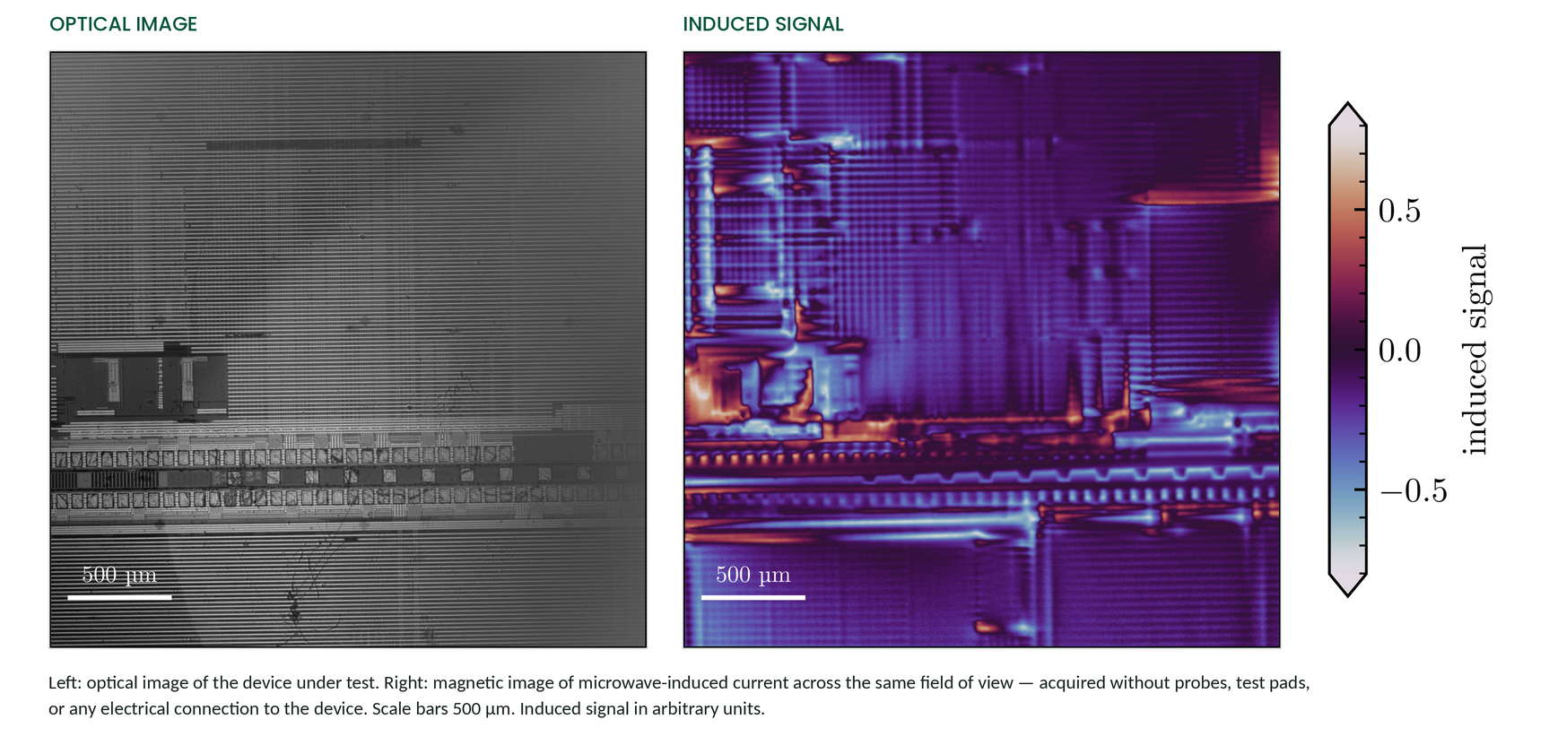
A production line cannot afford even that: every device would still need its own physical connection. That mismatch, rather than any limit of sensitivity, is what has kept electrical current imaging out of high-volume quality control. And for inline steps such as hybrid bonding process control, contactless excitation is the only option for measuring an unpowered, unfinished, mid-process wafer stack.
QD’s method excites current in the structure electromagnetically rather than galvanically, using microwave fields in place of a direct electrical bias. The induced currents produce magnetic fields, which QD’s diamond quantum sensors measure directly and reconstruct into a map of where current is, and is not, flowing.
The process addresses a specific gap. An interconnect can be geometrically sound and still fail to carry current. Inspection methods that image structure will pass it, while electrical testing reports only that the finished device is bad, without indicating where. Imaging the current itself is what connects those two results, and the need for it grows as hybrid bonding and stacked architectures bury more of the interconnect out of reach.
“Our approach gives you different information than other tools,” said Dr. Fleming Bruckmaier, CTO of QuantumDiamonds. “Acoustic imaging tells you whether a structure is mechanically sound. This tells you whether current is actually moving through it. Those are different questions, and a package can pass one and fail the other.”
The method inherently allows for mapping the 3D field vector of the induced current signature as seen by the diamond sensor. It can thus be used to reconstruct depth information similarly to QD’s established magnetic field sensing technology.
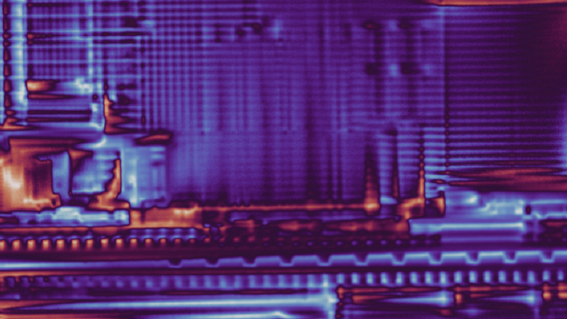
The measurement is made with the same diamond sensor head that QD ships in the QDm.1, its commercial failure-analysis system, which means the sensing hardware already working in FA labs can be carried into an inline configuration. The result is a whole-field image. In the comparison released today, a conventional optical view of a wafer region sits beside QD’s current image of the same area, which reveals a dense network of current pathways largely invisible to optical inspection.
The approach carries a characteristic trade-off. Because the excitation couples into the entire field of view at once, the technique images everything simultaneously and cannot isolate a single trace the way biasing a specific pad or pin can. For interrogating one known net, contacted measurement remains the more selective instrument. For surveying a structure with no electrical access at all, imaging the whole field in a single acquisition is the point.
Foundries and packaging customers are evaluating the technique now on their own die- and package level samples. QD has filed patent applications covering the method and is working toward the throughput a production environment requires.
QuantumDiamonds builds magnetic field imaging systems based on diamond quantum sensing for the semiconductor industry. Spun out of the Technical University of Munich in 2022, the company’s QDm.1 system images the magnetic fields produced by current flowing through a chip and reconstructs that current in three dimensions, non-destructively and without damaging the device.
For mor information: www.qd-st.com