Nikon Introduces Large-Stage Optical Measurement System for Advanced Packaging
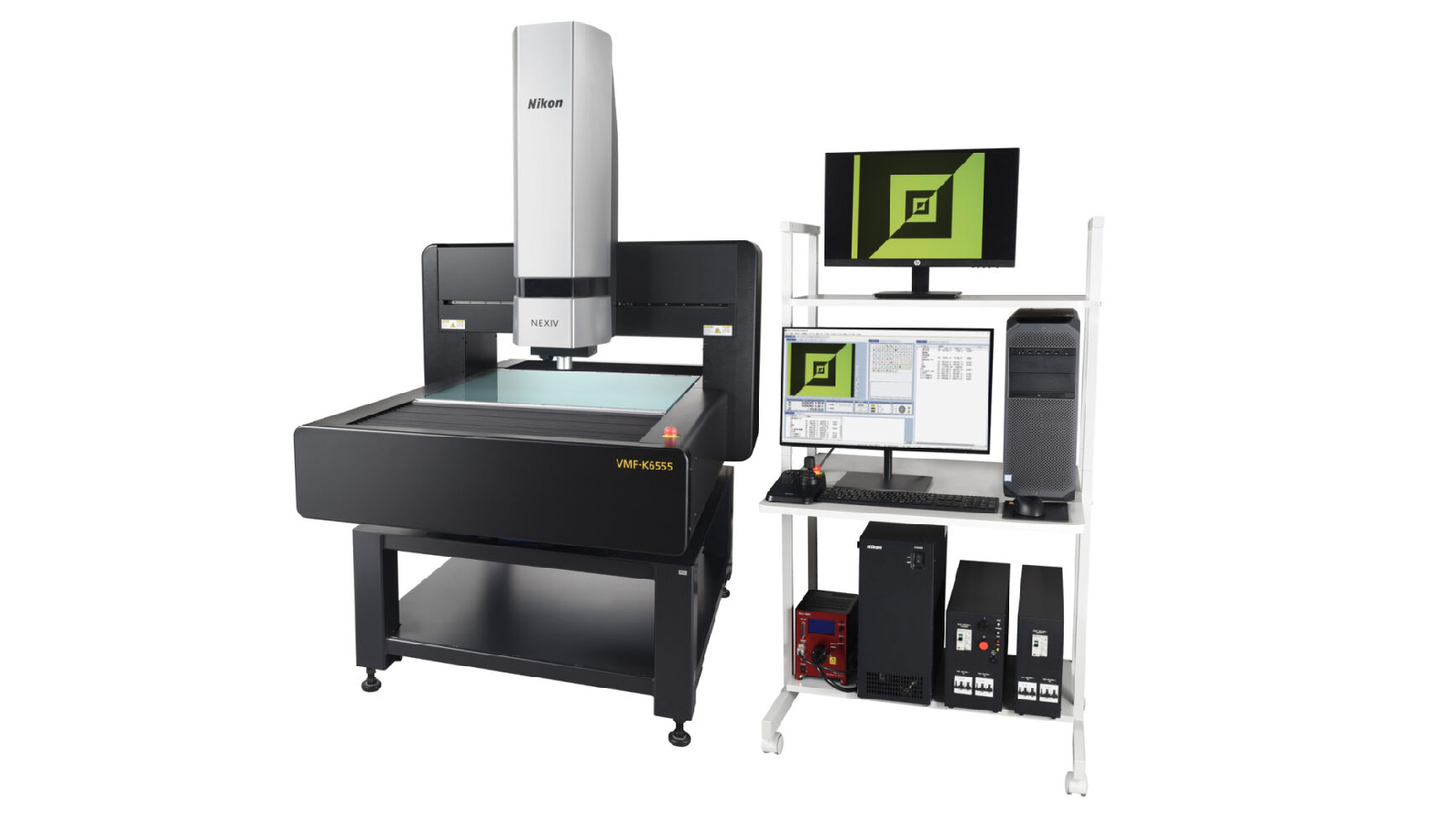
Nikon Corporation has expanded its NEXIV 3D Confocal series with the launch of the new NEXIV VMF-K6561, a high-speed optical measurement system designed to support the growing demand for large-format panel-level package (PLP) inspection in semiconductor and precision engineering applications.
Building on the proven capabilities of the NEXIV VMF-K series, the new VMF-K6561 introduces a 650 × 610 mm stage capable of accommodating and measuring complete 600 × 600 mm panels in a single setup. The enhanced stage size enables full-panel inspection of large panel-level packages while significantly reducing measurement times and eliminating the need for multiple repositioning steps during inspection.
The launch reflects increasing industry demand for faster, more accurate metrology solutions capable of supporting advanced packaging technologies and increasingly miniaturized semiconductor devices.
Designed for Large-Scale Panel Measurement
At the heart of the NEXIV VMF-K6561 is its newly engineered large-format stage, specifically developed for 600 × 600 mm substrates commonly used in advanced packaging applications. By enabling full-panel measurement in a single operation, the system helps manufacturers streamline inspection workflows, reduce production bottlenecks, and improve throughput in high-volume environments.
To maintain measurement stability across the larger inspection area, Nikon has also increased the thickness of the stage glass, helping ensure consistent accuracy and repeatability during operation.
The VMF-K6561 extends the capability of the existing VMF-K lineup, which combines high-speed 2D and 3D optical measurement technologies with confocal imaging to deliver precise dimensional analysis across a wide range of materials and geometries.
Advanced Confocal Technology for High-Speed Metrology
The NEXIV VMF-K Series is designed to overcome many of the challenges associated with traditional optical measurement systems. By incorporating an advanced confocal optical system, the platform enables rapid and highly accurate inspection of complex surfaces, including high-contrast materials, reflective components, and transparent substrates.
The integrated 2D and 3D measurement functionality allows manufacturers to perform detailed surface and height analysis within a single system, dramatically reducing inspection times compared with conventional metrology approaches.
This capability is particularly valuable in semiconductor manufacturing and precision engineering environments, where shrinking device geometries and increasingly complex package structures demand faster and more comprehensive quality control processes.
Supporting Next-Generation Semiconductor Packaging
As panel-level packaging continues to gain momentum across the semiconductor industry, inspection systems capable of handling larger substrates with high accuracy are becoming increasingly important. The VMF-K6561 addresses this requirement by providing stable, full-panel measurement capability for large-format PLP applications.
The system is also well suited for manufacturers working with miniaturized components and complex multilayer structures, where precise dimensional inspection is essential to maintaining process quality and yield.
Nikon says the enhanced optical measurement capabilities of the VMF-K Series enable reliable inspection of fine structures and challenging geometries that were previously difficult to measure efficiently using conventional systems.
For more information: industry.nikon.com