Quantum Diamond Microscopy – Solving the Inspection Gap in Advanced Packaging
Modern chip packaging has become one of the most demanding inspection challenges in any manufacturing environment. As the semiconductor industry shifts from single-die packages to chiplet architectures, 2.5D interposers, and vertically stacked 3D structures, the features that matter most for electrical performance are increasingly buried beneath layers that existing non-destructive tools were never designed to analyze. A new technique called quantum diamond microscopy (QDM), now entering commercial deployment in semiconductor laboratories across the US, Europe, and Asia, offers the industry something it has lacked: direct, non-destructive measurement of electrical current flow inside a fully assembled device.
A Gap the Existing Toolkit Cannot Close
The failure localization challenge is structural. Optical methods are the workhorse of electrical analysis – localizing defects with ~10 µm precision for higher resolution tools to be able to efficiently perform their job. But these optical techniques cannot penetrate completed package stacks. The two tools engineers rely on for subsurface insight, lock-in thermography (LIT) and X-ray computed tomography (CT), each address part of the problem but leave a critical gap between them.
Lock-in thermography is sensitive to heat. Where current encounters resistance, a temperature rise occurs, and LIT captures that thermal signal with high sensitivity. The difficulty is diffusion: in a single-layer package, thermal spreading is manageable, but in a multi-layer 3D stack, heat from a buried defect may disperse across adjacent structures before reaching the surface sensor, reducing a specific fault to an approximate warm region. In addition, the diverse material composition leads to highly anisotropic thermal spread, making LIT data unusable for localization in most deeply buried cases.
X-ray CT penetrates the full package and resolves physical geometry in three dimensions with outstanding fidelity. Voids, delaminations, cracks, and physical discontinuities are all visible. But X-ray contrast is structural, not electrical, while taking a substantial amount of time per measurement. A microbump that is mechanically intact but electrically open, due to a marginal adhesion failure, a delaminated interface layer, or a grain boundary that is physically closed but electrically discontinuous, is indistinguishable from a good bump. The failure is invisible precisely because the structure appears normal. Furthermore, one of the most sensitive types of chips, memory, is ubiquitous in modern packages – and easily gets irreversibly damaged by the high-energy X-rays used in failure analysis.
The architectures driving this complexity, including 2.5D interposer platforms such as CoWoS, silicon bridge technologies such as EMIB, and fully stacked 3D configurations, all share the same vulnerability: electrically critical interfaces buried beneath layers that conventional tools cannot properly inspect. As Fleming Bruckmaier, CTO and co-founder of QuantumDiamonds, puts it: “Magnetic imaging is the tool missing in the FA toolkit, to actually tackle the packaging paradigm shift that is happening.”
A Different Physical Principle: Measuring Current Directly
Quantum diamond microscopy addresses this by measuring something different altogether: the magnetic fields generated by current flowing inside the device. Every conductor carrying current produces a magnetic field, a consequence of basic physics that holds regardless of whether the conductor is dissipating power or is structurally intact. By imaging those fields at micrometer spatial resolution, QDm reconstructs a map of where current is flowing and, critically, where it is not.
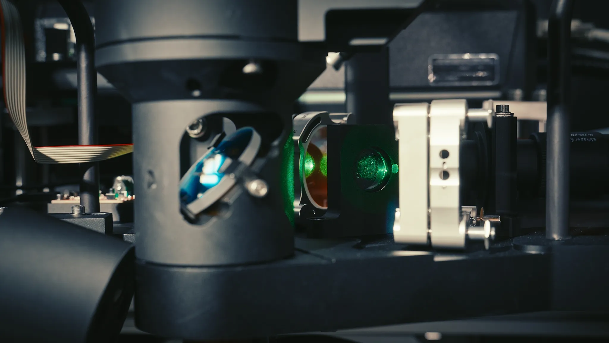
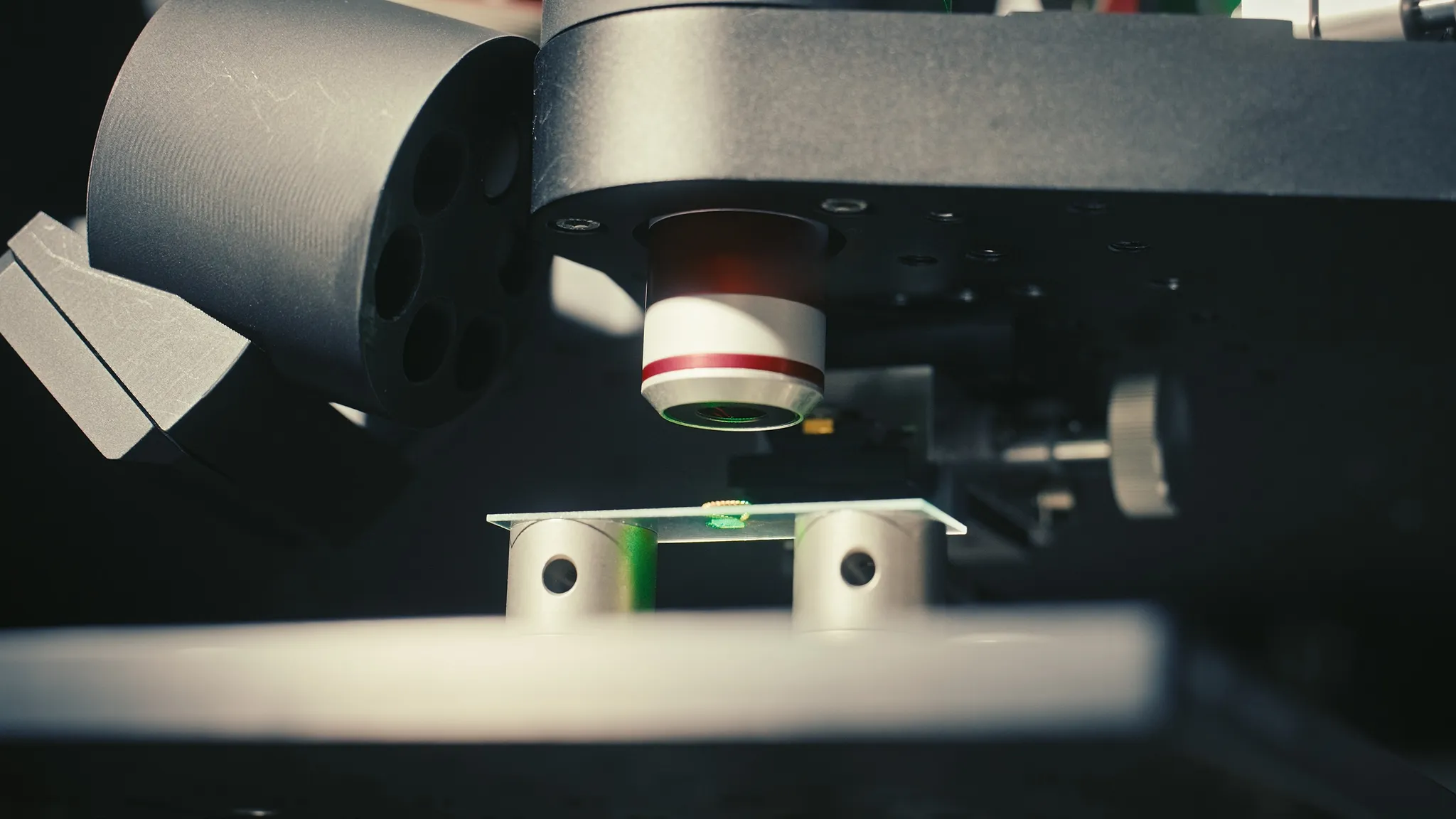
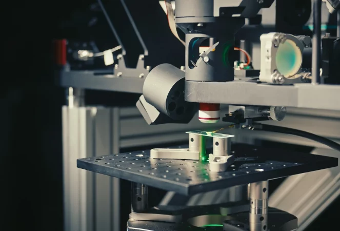
The sensing mechanism depends on a specific defect in synthetic diamond. Nitrogen-vacancy (NV) centers are atomic-scale defects intentionally created in a thin layer of laboratory-grown diamond. Each NV center acts as an extremely sensitive local magnetometer: its quantum state shifts measurably in response to the magnetic field at its location. Illuminating the NV layer with a green laser and reading out the resulting optical signal recovers a spatially resolved magnetic field map across the entire field of view simultaneously, a widefield image rather than a point-by-point scan. QDm comes with all the advantages of optical imaging: resolution, speed and ease of use, without requiring optical access to the defect location.
In operation, the synthetic diamond sensor chip is placed against the surface of the device under test. A bias current is applied, replicating the conditions under which the failure is observed, and the instrument acquires a full magnetic field map of the package beneath. A current reconstruction step converts that magnetic map into a two-dimensional current density image, showing which conductors are carrying current and which are not. The output overlays directly onto the chip’s layout database, allowing the engineer to identify immediately which interconnect, TSV, or microbump is anomalous. The measurement requires no vacuum, no cryogenic cooling, no sample preparation, and no mechanical modification of the device. The chip goes in, the measurement runs in seconds to minutes, and the chip comes out intact.
The diagnostic significance lies in what magnetic current imaging reveals that thermography and X-ray cannot. A partial open at a microbump or TSV, where contact resistance has increased significantly but continuity has not been entirely lost, may pass room-temperature electrical test while causing intermittent failure under stress. In a thermal image, the resistance may be too small to generate detectable heat. After using X-ray, the chip is likely permanently damaged. In a current map, however, the redistribution of current around the high-resistance path creates a distinctive anomaly that points directly to the fault location, without any damage to the device. Similarly, current leakage paths between adjacent conductors appear as unexpected current concentrations in the QDM map even at levels too small to trigger in-line leakage tests. Backside power delivery network defects, increasingly relevant as logic manufacturers move power delivery to the other side of the wafer, are directly assessable through the full package thickness without destructive layer removal.
From Fault Confirmation to Root Cause in a Single Session
A published case study illustrates the workflow advantage. In a study by QuantumDiamonds involving commercial integrated fan-out package-on-package (InFo-PoP) devices, a short-circuit failure was suspected on the package backside. Lock-in thermography confirmed the failure and identified the approximate position at the millimeter scale, but thermal diffusion made precise localization impossible. X-ray CT confirmed structural integrity with no visible discontinuities. Without a more precise fault location, the failure analysis team faced systematic deprocessing and cross-sectioning of the entire suspected region, a process that can take days and risks destroying root-cause evidence before it is identified.
QDM was applied with a bias current replicating the failure condition. The resulting current map showed a redistribution anomaly consistent with a power-to-ground short circuit, localized to a region of approximately 20 x 20 microns in a component on the backside. FIB cross-sectioning directed to that location confirmed root cause on the first attempt, a processing anomaly at an integrated passive device interface, without iterative deprocessing. What would typically require multiple days of systematic analysis was resolved in a single session.
From the Failure Analysis Lab to the Production Line
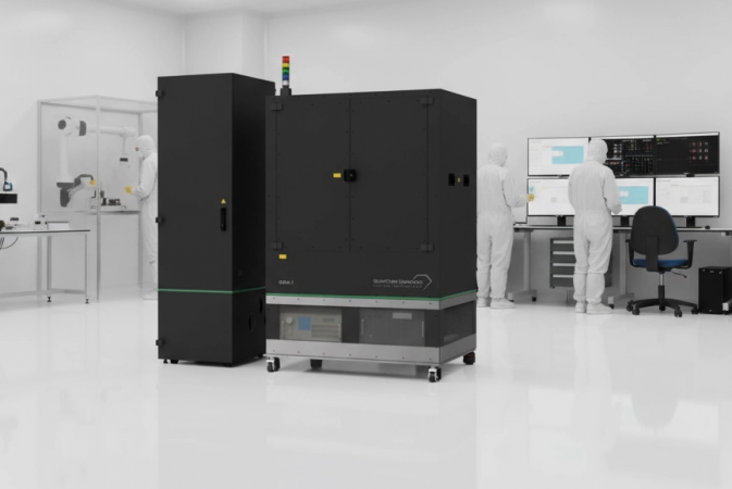 QuantumDiamonds has commercialized QDM as the QDm.1, the first integrated quantum sensing system designed for semiconductor failure analysis. The system is now in active deployment at leading failure analysis laboratories in Europe, Asia, and, following the company’s first North American installation at Eurofins EAG Laboratories in Sunnyvale. They are part of the growing recognition of NV-diamond magnetic imaging as an important semiconductor characterization technique, which is reflected in peer-reviewed literature, conference programs, and emerging commercial activity.
The product roadmap extends the technique progressively closer to the production line. The current InLab configuration is positioned as a failure analysis and process debug tool. An InFab configuration targeted for 2027 is designed for lot-level defect metrology at advanced packaging lines with throughput compatible with sampling inspection. An InLine wafer-level configuration, targeted for 2028, aims to enable 100%, non-contact, in-line current mapping at key assembly process steps. The trajectory follows a path familiar from the history of semiconductor metrology: a technique that begins in the failure analysis laboratory migrates toward the production line as throughput improves and the economic case for in-line deployment becomes compelling.
The broader significance is the addition of electrical inspection at depth to a measurement toolkit that has historically been limited to structural and thermal dimensions. For process engineers qualifying new packaging processes, including hybrid bonding at sub-5 µm pitch, chiplet integration in large-format packages, and backside power delivery in advanced logic, QDM provides direct observation of current distribution in assembled devices without destruction. For failure analysis engineers, it changes the economics of buried-defect investigation. For quality engineers, the roadmap toward in-line current mapping represents a long-term prospect of 100% electrical integrity screening at the package level, closing the detection gap between wafer-level electrical test and customer returns.
As package complexity increases and buried interconnect density grows, the fraction of yield-limiting failures that are electrically active but structurally invisible will grow with it. Magnetic imaging through diamond quantum sensing opens a new measurement window, one that sees not the geometry of the device, but the current flowing through it.
For more information: www.qd-st.com