Optical Inline Quality Assurance for Electronics Manufacturing
World First HoloTop Motion: 3D Measurement Without Downtime
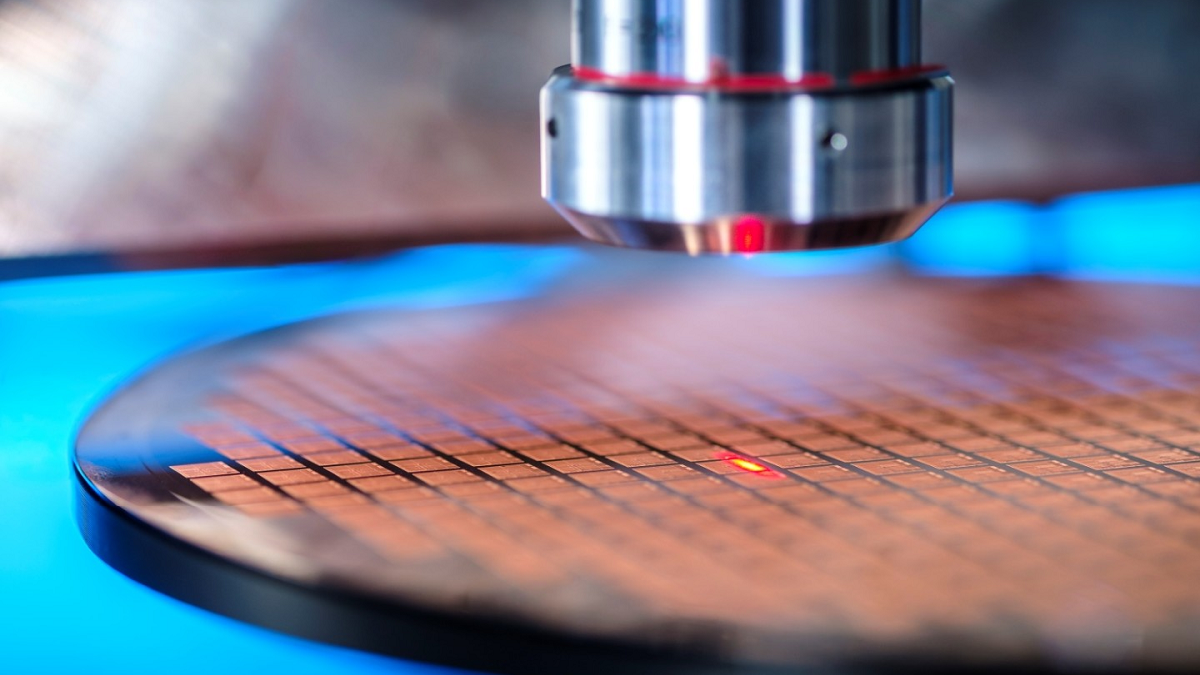
With HoloTop Motion, Fraunhofer IPM presents for the first time a new generation of digital holographic sensors for the high-precision 3D measurement of moving surfaces. Unlike conventional methods, the components do not need to be stopped or removed from the production line for measurement. The sensor captures the surface strip by strip and combines the measurement data into a continuous topographic measurement.
The system is particularly suitable for inspecting wafers, interposers, or ball grid arrays. Depending on the lens used, HoloTop Motion achieves a lateral resolution of better than two micrometers. Axial reproducibility is less than one micrometer. Measurements are possible at feed rates of up to one meter per second.
F-Camera Detects Contamination on Electronic Contacts
Clean surfaces are essential for reliable electrical welding, soldering, plugging, and crimping connections, as well as for subsequent joining, coating, or bonding processes. Even minute residues of oils, greases, cleaning agents, lacquers, or fluxes can impair the quality and function of electronic components. The F-Camera inspects surfaces using imaging technology and without physical contact, integrated into the production cycle. UV light stimulates organic substances to fluoresce, making even minute residues visible and quantifiable. The system captures, among other things, the position, shape, and extent of contaminants and defects.
RAPID-LIBS Controls Laser Drilling of Microvias
Microvias connect the conductive layers of multilayer printed circuit boards. Laser drilling requires the precise removal of insulating material without damaging the underlying copper layer. However, fluctuating layer thicknesses make it difficult to reliably control the laser process with a fixed number of laser pulses. RAPID-LIBS analyzes the plasma generated during laser ablation. The system captures its material-specific spectrum and identifies in real time which material is currently at the processing point. Material transitions can be resolved pulse by pulse and immediately fed back to the laser controller as a control signal. This allows each hole to be individually controlled in real time.
For more information: www.ipm.fraunhofer.de