
Scanning Acoustic Tomograph Enables Higher Defect Detection Image Quality
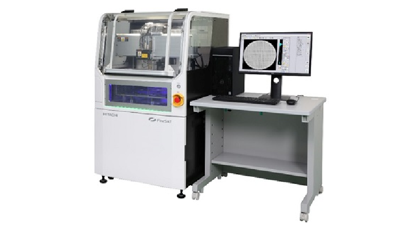
Hitachi Power Solutions has announced the launch of its Scanning Acoustic Tomograph ‘FineSAT7’ as the newest model of the FineSAT series that detects and images minute structures and defects such as delamination and voids inside semiconductors and electronic components non-destructively by utilizing the reflective and transmissive properties of ultrasonic wave. The system enables high-quality defect-detection images and one-time inspection of 300 mm wafers by adopting an A/D conversion board with the resolution by 16 times and the measuring period by twice compared to the conventional model. FineSAT7 which contributes to improve inspection accuracy and productivity in research, development, and manufacturing fields through these performances and functions.
Background of Development
 As semiconductor devices, electronic components, automotive devices and power devices have been manufactured in more miniaturized size in recent years, higher-quality inspections are required by manufacturers. In addition, there is an increasing need for one-time inspection using the through transmission method in view of work-efficiency and productivity, because defect inspection for each layer is required for products with multi-layered structure, such as 2.5D and 3D. For wafer inspection, which is material of semiconductor devices, there is also an increasing need for equipment compatible with inspections of large-size wafers used for mass production.
Hitachi Power Solutions has a wealth of experience in the domestic and overseas market, including sales of approximately 2,400 units of FineSAT series as a non-destructive device for detecting and imaging microscopic structures and defects inside semiconductor devices and electronic components by utilizing the reflective and transmissive properties of ultrasonic waves.
Maximum Scanning Speed 2,000 mm/second
When measuring a large sample the measurement time is largely affected by the scanning speed. The measurement time is shortened by 25% by reducing the ultrasonic pulse generation cycle by half in addition to using a high-speed scanner. The maximum scanning speed of the scanner excluding acceleration and deceleration time has improved to 2,000 mm/s. The newly designed highly-rigid frame suppresses equipment vibration, producing crisp images even from high-speed scanning.
A larger water tank realizes one-time inspection of 300 mm wafers using the through transmission method. Conventionally, inspection of 300 mm wafers had to be performed half-side by side while moving the inspection object.
For more information: www.hitachi-power-solutions.com

