
OPTOCOMB’s Unique Metrology Capabilities at Core of Nikon’s Next Big Thing
The OptoComb is a high-precision measurement technology that has been developed by XTIA Ltd., a high-tech company spun off from the Tokyo Institute of Technology. Nikon already possesses world-class optical and precision technologies, but it is now taking on the challenge of launching new business using the world’s most advanced technologies. XTIA has been chosen as a partner of choice in this endeavor and it is currently accelerating its cooperation with Nikon.

The two companies aim at leveraging their mutual strengths to target new markets and develop the next revenue stream. The key person behind this initiative, Kaneyuki Naito – Manager of the Development Section of Nikon’s Next Generation Project Division, explains the attraction of OptoComb technology to Nikon.
Q: Please tell us about the new business you are working on.
A: Nikon has two core businesses: the imaging business, which handles digital cameras, and the precision equipment business, which handles lithography equipment. The Next-Generation Project Division, of which I am a member, is responsible for launching advanced products that will become the brand-new cores of Nikon’s business.
The Next Generation Project Division was launched in 2019 as a spin-out from the Semiconductor Lithography Equipment Development Department, a department that develops equipment with the world’s top-class precision. We started with the idea that we could provide new and unique value by combining Nikon’s world-class optical technology and the ultra-precision control technology we have developed for our semiconductor lithography equipment. What we created was a material processing solution fully based on light. I have been overseeing not only the development of the technology, but also the launch of a brand-new business based on such a light-based material processing technology.
Conventional machining processes cause distortion due to thermal effects and cutting resistance, whereas microfabrication is expensive. Nikon’s optical processing equipment makes it possible to achieve distortion-free microfabrication at low cost. In addition, Nikon’s optical processing equipment can process complex shapes and difficult to access areas that drills cannot penetrate, and it can be used in a wide variety of materials, making it useful in many different fields. Leveraging this unique light-based technology, Nikon is committed to launching a new and unparalleled material processing business.
Q: Tell us about your encounter with XTIA and its OptoComb technology.
A: In the process of commercializing light-based material processing, we were faced with a major challenge in that we did not have sufficient
technology to measure the object to be processed at high speed and with high precision. Ultra-precise processing cannot occur without ultra-precise measurement of the object. Optical processing is done by focusing a laser with a lens, and to use an analogy, it is the same as the way a magnifying glass collects light on a piece of paper. If your hand is shaky, the paper will not burn. In optical processing, too, it is important to focus the light precisely with micron-order precision.
We first learned about XTIA when comparing various advanced technologies through discussions with the University of Electro-Communications, Japan, and other institutions with deep knowledge of the optical comb technology. XTIA has been the first company to put the optical frequency comb technology to practical use for industrial applications, and they are now playing a central role in our new business development, supporting us in our next-generation endeavors.
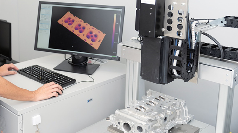
Q: How is the OptoComb technology being used for 3D metrology?
A: One example is a biomimetic technology called ‘riblets’. Riblets are microscopic groove structures ranging from several 10s to 100 microns in size, that are present on the skin of sharks and allow them to swim faster. By machining such microscopic grooves on surfaces that come into contact with fluids such as air and water, surface friction resistance can be reduced, resulting in improved energy efficiency and reduced CO2 emissions.

One example would be the machining of airplane fuselages and gas turbine blades. These are very large workpieces and micromachining can vary slightly from piece to piece: with the OptoComb technology, the shape of the piece can be measured at high speed and high accuracy in order to highlight and correct such variations. Furthermore, since both the OptoComb technology and optical processing machines use light, a completely new concept of ‘co-axial measurement and processing’ has been created.
The OptoComb measurement laser is superimposed on the laser used for processing, and both lasers are directed to the object to be processed. By extracting only the OptoComb signal from the light reflected by the object, it is possible to measure the point that is being processed. Conventional measurement methods sometimes hide the machining area, but with such a coaxial process measurement, the entire machining area can be accurately measured. We were able to quickly build the prototypes we were looking for, which allowed us to quickly demonstrate this concept. Several optical machining centers using coaxial measurement machining have already been realized, and we are considering further applications of this technology.
OptoComb technology can lead to great innovation for manufacturers around the world.
For more information: www.optocomb.com

