
Covalent Metrology Expands Scanning Electron Microscopy Capabilities
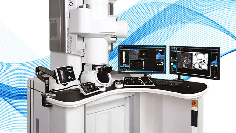
Covalent Metrology, a North-American analytical services provider, has announced that it has significantly expanded its capacity and capabilities for (Scanning) Transmission Electron Microscopy (S/TEM). The JEM-F200 S/TEM from JEOL, a manufacturer of analytical instruments based in Japan, streamlines analysis and permits more flexible sample types, including beam-sensitive and magnetic materials. Clients working with semiconductors, batteries, nanomaterials, and more will benefit from atomic-scale imaging and EDS mapping, along with new energy-filtered TEM (EFTEM) and high-resolution EELS services that can help to design, optimize, and accelerate manufacturing processes.
The CFEG and advanced optics in the tool provide exceptional beam stability and performance. High spatial resolution, high current, and narrow energy spread on the tool produce atomic-scale resolution for both imaging and spectroscopic analysis.
The narrow energy spread additionally facilitates high energy resolution (0.3 eV) for EELS and EFTEM on the equipped Gatan GIF Continuum ER system. EELS enables elemental composition mapping, low-loss and plasmon resonance analysis, and fine-structure/oxidation state determination for nanoelectronic materials. EFTEM provides significant benefits for analyzing light-element materials, allowing Covalent to address many common challenges in battery and memory devices.
The JEM-F200 also substantially improves Energy Dispersive X-ray Spectroscopy (EDX/EDS), with paired detectors working simultaneously to accelerate collection times. Rapid spectroscopic analysis and high current from the CFEG preserve high spatial resolution at low-dose conditions (below 2 Angstroms at 80kV) for beam-sensitive materials, such as those used in photovoltaics.
“Covalent is thrilled to enhance our S/TEM microanalysis capabilities and to better serve clients in advanced research communities, which demand atomic resolution for complex device structures, light element analysis, and nanoscale defects,” says Dr. Yihung Lin, Vice President and Head of Analytical Services at Covalent Metrology. “Bringing EELS in-house and expanding our TEM capacity will reduce turnaround time and expand our solutions for clients working with semiconductors, batteries, or nanomaterials.”
The JEM-F200 installation marks another step forward in Covalent’s partnership with JEOL. Covalent has already installed the JCM-IT800HL high-resolution SEM, a JCM-7000 benchtop SEM, and an IB-19520CCP ion-mill cross-section polisher in its Silicon Valley lab.
Bob Pohorenec, President of JEOL USA, noted, “The installation of the JEM-F200 in our joint demo facility with Covalent positions JEOL to better showcase the breakthrough capabilities of the tool throughout the West Coast of North America. This location and the unique applications development at Covalent allow us to demonstrate the microscope’s potency in a variety of industries based in the Silicon Valley and beyond.”
For more information: www.covalentmetrology.com


