Nearfield Instruments Launches Sidewall Imaging Mode for Inline 3D Semiconductor Metrology
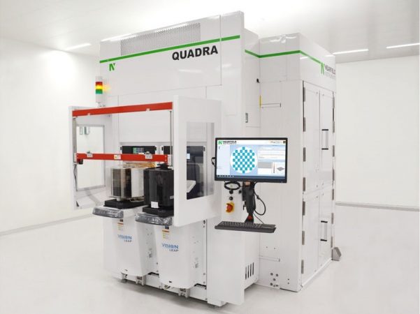
Nearfield Instruments, a leader in advanced semiconductor metrology and process control, has announced the launch of its new Sidewall Imaging Mode, a measurement breakthrough for its QUADRA high-throughput scanning probe metrology platform. The mode provides non-destructive, inline 3D sidewall profiling for high-aspect-ratio features in advanced logic and memory devices. Sidewall imaging gives chipmakers the ability to monitor next-generation semiconductors with unprecedented precision during process development and high volume manufacturing.
Non-Destructive 3D Metrology of Three-Dimensional Structures
 As artificial intelligence (AI) drives explosive growth in global compute demand, the semiconductor industry has transitioned from flat, two dimensional device architectures to fully three-dimensional structures such as gate-all-around (GAA), complementary FET (CFET) roadmaps, and 3D memory architectures. In these architectures, device performance is increasingly defined by the shape and quality of the vertical structures. Sidewall angle, roughness, and uniformity directly influence variability and leakage of 3D chips. At leading-edge nodes, a systematic 0.1 nm bias in critical transistor dimensions already leads to a much less energy-efficient chip, which costs a hyperscale data center operator terawatts per year, the equivalent of hundreds of millions of dollars in additional electricity costs.
Today, detailed sidewall information is primarily obtained through transmission electron microscopy (TEM), the industry’s reference standard for 3D structural analysis. While TEM delivers extremely high resolution insight, cross-sectional TEM depends on lamella extraction and thinning, which takes the sample out of the standard production flow and inherently limits sampling volume and throughput.
 The patented Sidewall Imaging Mode is designed to complement these techniques by bringing 3D sidewall information inline, enabling statistically robust datasets for statistical process control (SPC) and rapid process optimization. By making third-dimension control practical at scale, the technology supports faster innovation cycles, higher manufacturing yield, and the production of more energy-efficient AI chips.
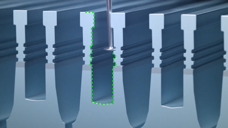
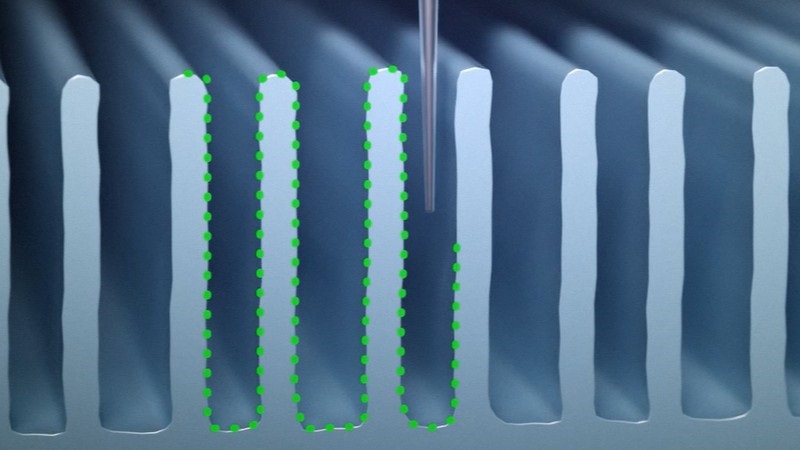
Sidewall Imaging Mode extends atomic force microscopy (AFM) using Nearfield’s patented cantilever design, sensor fusion, and trajectory control to capture both vertical and lateral interaction forces. This enables full 3D reconstruction of high-aspect-ratio features such as etched gates, nanosheets, and deep memory channels.
“The road to scaling compute performance is vertical, no matter the device. As devices move fully into the third dimension, process control must do the same. Sidewall Imaging Mode enables non-destructive 3D metrology with enough data to support both manufacturing precision and energy-efficient performance. This capability is fundamental for the next generation of AI-driven semiconductor technologies” saidDr. Hamed Sadeghian, Co-Founder and CEO of Nearfield Instruments.
For more information: www.nearfieldinstruments.com