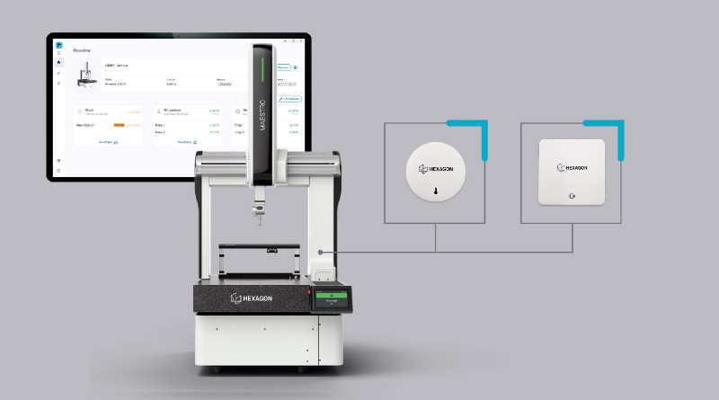
Upgraded PULSE Delivers Advanced Real-Time Environmental Monitoring for Shop-Floor Metrology
Hexagon’s Manufacturing Intelligence division has announced an evolved version of PULSE, its real-time environmental monitoring solution for coordinate measuring machine (CMM) environments, designed to help manufacturers improve measurement quality and reliability.
Read Article →