ZEISS Microscopy Spotlights Advanced Failure Analysis Technologies at ISTFA
ZEISS Microscopy will once again make a strong showing at the 51st annual International Symposium for Testing & Failure Analysis (ISTFA), taking place November 16-20, 2025, at the Pasadena Convention Center, in Pasadena, California.
ZEISS will deliver seven papers and two tutorials showcasing its expertise in a wide range of imaging applications, techniques and correlative methodologies for semiconductor failure analysis (FA). The papers will focus on topics covering AI-based image segmentation, automation, power devices, hybrid bond analysis, and more. ZEISS experts will also participate in the Tools of the Trades Tour.
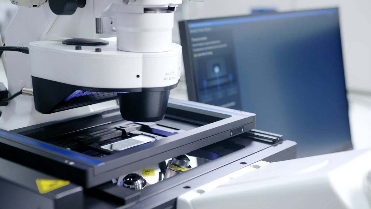
ZEISS will share the latest advances in 3D X-ray microscopy, FE-SEM, and FIB-SEM solutions for FA and process development. Visitors can learn about key products, including ZEISS VersaXRM 730 X-ray microscope, ZEISS GeminiSEM FE-SEM (including new 200 mm chamber option), ZEISS Crossbeam FIB-SEM, and ZEISS Crossbeam Samplefab systems.
“As microscopy becomes more intelligent with the use of AI and interconnected through multiple modalities, its role in advancing innovation across the electronics industry grows exponentially. ISTFA provides an ideal platform to demonstrate how ZEISS solutions are driving precision and efficiency in materials characterization and failure analysis,” said Dr. Thomas Rodgers, Head of Business Sector Industry at ZEISS Microscopy. “At ISTFA 2025, we’re highlighting how advancements in areas such as automation, AI, and correlative technologies are shaping a new era of insight, enabling engineers to push the limits of design and reliability.”
For more information: www.zeiss.com/microscopy