Surfmera Atomic Force Microscope Lineup Unveiled
Surfmera has announces its advanced suite of atomic force microscopes (AFM), positioning the company as a leader in nanoscale imaging and measurement solutions. Designed to empower researchers and industries, these cutting-edge instruments unlock new dimensions in material properties, chemical composition, and physical phenomena at the atomic and molecular levels. By combining robust engineering with user-centric software and automation, Surfmera’s platforms transform complex nanoscale analysis into efficient, reproducible, and insightful workflows.
 Surfmera’s commitment to performance, accessibility, and reliability ensures that its instruments meet the most demanding requirements of academic and industrial users worldwide. Whether for fundamental scientific discovery or optimizing high-volume production processes, these AFMs provide unified, robust, and intuitive platforms that deliver not just data, but clarity.
Applications span material science, including nanostructures, 2D materials, semiconductors, thin films, polymers, energy materials, and metamaterials. It also excels in electromagnetic characterization with techniques like Kelvin Probe Force Microscopy (KPFM) for surface potentials (3mV sensitivity, 20nm resolution), Electrostatic Force Microscopy (EFM), Piezoresponse Force Microscopy (PFM), Conductive AFM (C-AFM) with pA sensitivity, and Magnetic Force Microscopy (MFM). For life sciences, it supports multi-environment imaging in air or liquid with precise temperature control, quantitative nanomechanical analysis of cell elasticity and adhesion, and diverse applications from single-molecule biophysics to live-cell dynamics.
Core of Nanolab
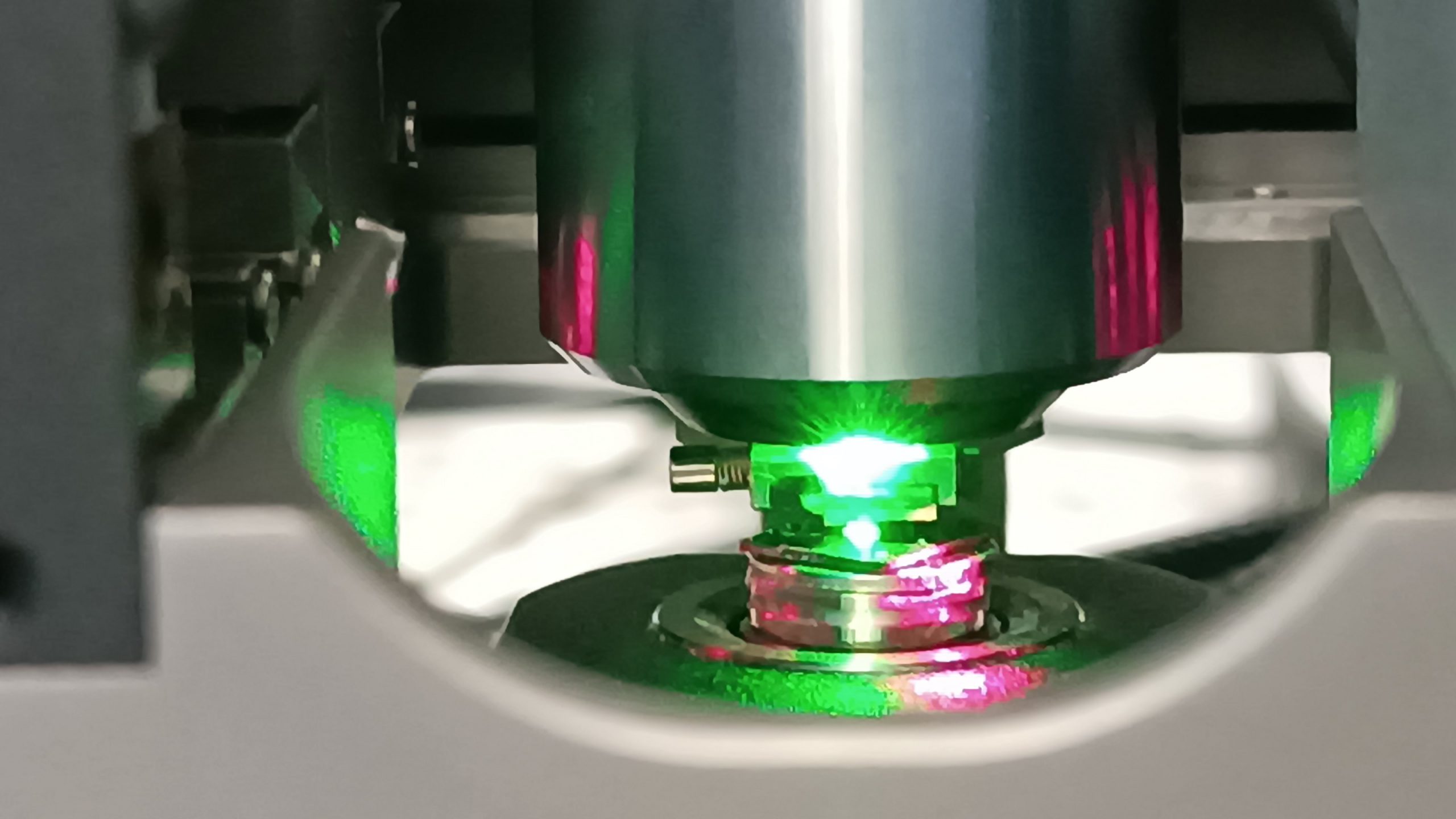
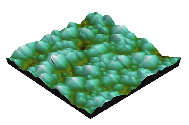
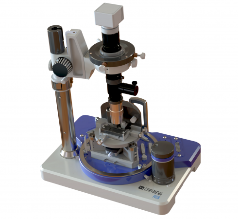 At the heart of Surfmera’s offerings is the AXIS Foundation, a universal platform engineered for unbeaten flexibility and professional-grade performance in scanning probe research. Key features include an open design for easy sample access, over 50 standard AFM modes with customizable software, scalable expansion to AFM-Raman-TERS or AFM-nano-IR, versatile environments (vacuum, controlled atmosphere, or fluid), and precise quantitative nano-mechanical measurements with artifact-free scanning.
The AXIS Lumina integrates high-end AFM with confocal Raman and Scanning Near-field Optical Microscopy (SNOM) for sub-10nm chemical, structural, and mechanical mapping. It features in-situ environment control in air, liquids, controlled atmospheres, and variable temperatures; modular design with up to five interchangeable lasers and multiple illumination paths; and automated workflows for intuitive data acquisition and analysis.
Ideal for nanoscale analysis, it combines AFM topography with Raman spectral mapping to reveal defect distributions, strain effects, and interlayer interactions in graphene, TMDs, and van der Waals heterostructures. Additional modes include Tip-Enhanced Raman Scattering (TERS) for sub-diffraction chemical imaging with plasmonic optimization and polarization control; polymer and composite investigation for phase separation and filler distribution; and optical device characterization for photonic components like semiconductor lasers and plasmonic structures.
Bridging Research Bench to Production Line
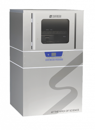 Surfmera’s Proxima serves as an industrial nanoscale analysis workhorse, merging lab-grade precision with smart production-line automation. It offers nanometer-scale precision in industrial environments, AI-enhanced workflows for faster R&D cycles, and over 50 integrated techniques for comprehensive characterization. The system supports large samples with unmatched stability, transforming complex research into fast, reproducible workflows.
Key applications include precision wafer roughness inspection with comprehensive 200x200mm scanning, automated SEMI/ISO-compliant analysis, and 3D roughness maps; comprehensive morphological analysis of micro- and nanostructures with sub-nanometer resolution 3D characterization; and photoresist performance analysis for lithography optimization, measuring exposure dose effects on 3D morphology.
AXIS Infra: Apex of Nanochemical Insights
Building on its modular approach, the AXIS Infra platform combines AFM with Nano-IR for correlated nanoscale vision and analysis. It provides sub-10nm spatial resolution for optical mapping, over 40 AFM modes with broad spectral range coverage, multimodal capabilities for confocal Raman and TERS upgrades, and streamlined research for efficient, accurate results.
Applications focus on advanced material analysis through high-resolution chemical mapping. They are used to study polymer characteristics such as composition, phase separation, crystallinity, and degradation. In semiconductors, they enable high-resolution defect characterization and dopant distribution analysis. For metamaterials, the system provides comprehensive characterization of morphological, conductive, chemical, and optical properties under dynamic temperature control.
Surfmera’s Spark democratizes nanoscale research by combining research-grade precision with exceptional ease of use in a compact design. It features intuitive operation for all skill levels, a 100×100µm closed-loop scanner with sub-nanometer accuracy, a comprehensive suite of techniques (C-AFM, MFM, KPFM, PFM), and an adaptive interface with guided workflows for beginners and full manual control for experts.
For more information: www.surfmera.com