Revolutionizing Defect Detection – Next-Gen e-Beam Inspection Poised for Production
In a move that could reshape semiconductor inspection and metrology, it has been announced that Kioxia Iwate Corporation will begin evaluating a groundbreaking GaN (Gallium Nitride)-based e-Beam inspection and metrology technology in late September. The system has been jointly developed by Nagoya University startup Photo electron Soul Inc. and the Amano-Honda Laboratory at Nagoya University.
The field test will focus on validating the advantages of this next-generation inspection technology in advanced 3D NAND flash memory manufacturing, where defect detection and precise metrology are becoming increasingly critical to yield improvement. Kioxia Iwate will assess whether the technology can enhance defect identification and root-cause analysis directly within live production inspection processes.
What is an E-Beam Inspection System?
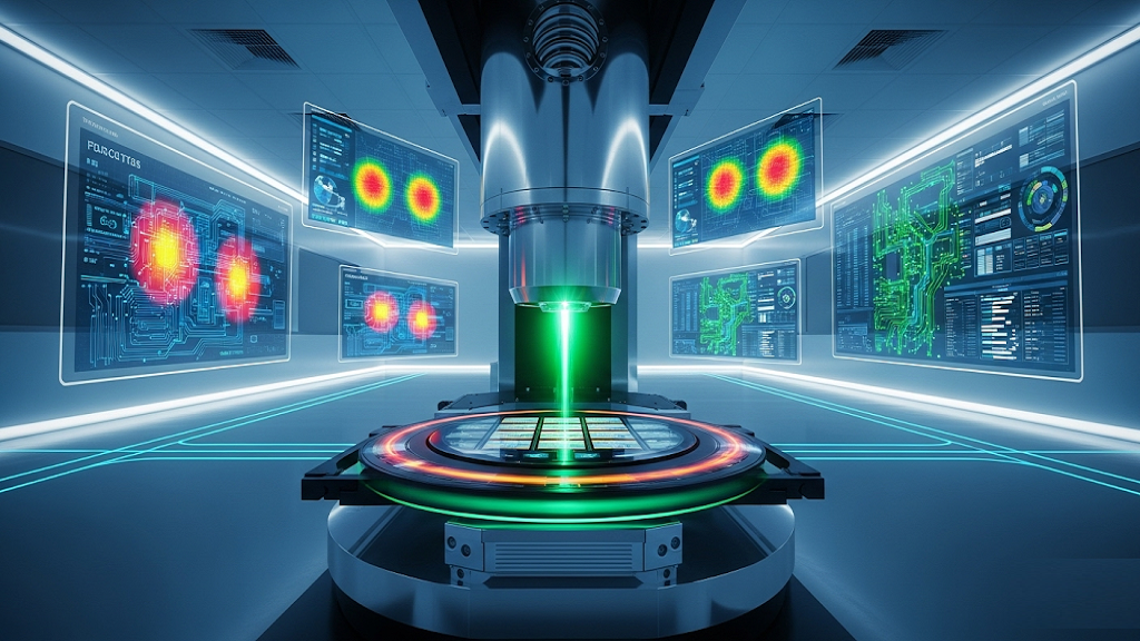
Electron beam (e-Beam) inspection systems are widely regarded as one of the most advanced quality control tools in semiconductor manufacturing. They use a high-energy beam of electrons to scan wafers, generating highly detailed images that can be analyzed for defects or imperfections. Unlike traditional inspection methods, e-Beam inspection is non-destructive and contact-free, making it well suited for fragile and miniaturized semiconductor structures.
When inspecting wafers, the system directs an electron beam onto the surface of the die. As electrons interact with the material, they scatter and are collected by detectors, producing an image of the surface and subsurface. This process allows engineers to identify surface imperfections, cracks, voids, material porosity, and subsurface defects that would otherwise go unnoticed.
The inspection process is powered by two key signals:
- Secondary electrons, which reflect off the wafer surface and provide fine surface detail.
- Backscattered electrons, which penetrate deeper into the material and reveal subsurface information.
By combining these signals, e-Beam inspection systems deliver an unmatched level of accuracy and precision, helping semiconductor manufacturers maintain consistent product quality while pushing device architectures to new limits.
However, conventional e-Beam systems face trade-offs. Their throughput is limited, often measured in square millimeters per hour, in contrast to optical tools that are evaluated by wafers per hour. This bottleneck means that while e-Beam systems provide exceptional accuracy, their use has traditionally been limited to sampling inspection rather than full production-scale monitoring.
Tackling the Complexity of 3D Flash Memory
The emergence of 3D NAND flash memory, with its vertically stacked cell architecture, has amplified the demand for advanced inspection and metrology. As layer counts increase and integration grows more complex, defect detection and dimensional metrology at the nanoscale become increasingly difficult.
Traditional optical or mechanical inspection methods struggle to probe deep, high-aspect-ratio structures without distortion or physical interference. This is where GaN-based photocathode e-Beam inspection and metrology, developed by PeS and Nagoya University, offers a significant breakthrough.
The GaN-Based Breakthrough
The technology under evaluation by Kioxia integrates two key innovations:
- Photocathode e-Beam Inspection – Enables non-contact electrical inspection and highly accurate defect detection in challenging deep-structure regions.
- Photocathode e-Beam Metrology – Provides profile measurement capabilities in areas inaccessible to conventional methods.
At its core, the system leverages the unique properties of GaN-based photocathodes, which allow for higher efficiency electron emission and more controlled beam characteristics. These enable novel capabilities, including:
- DSeB (Digital Selective e-Beaming): Targeted e-Beam radiation for selective inspection.
- YCeB (Yield Controlled e-Beaming): Real-time beam intensity control to prevent misalignment and ensure consistent accuracy.
Together, these innovations overcome the traditional throughput and precision limitations of conventional e-Beam systems, offering the promise of production-ready, high-resolution inspection within live manufacturing environments.
A Step Toward Commercialization
The upcoming evaluation at Kioxia represents a major milestone for Photo electron Soul.
“This evaluation provides a great opportunity for us to prove that our inspection and metrology technology is unmatched. No other inspection tool supplier has yet commercialized it, and it is ready for production in a semiconductor manufacturing environment,” said Takayuki Suzuki, CEO of PeS.
Suzuki emphasized that the adoption of this technology could provide Kioxia with a decisive competitive edge:
“We are confident that this will become a core technology for Kioxia, enabling them to significantly enhance their advanced inspection and metrology capabilities and outperform rival NAND flash producers in Korea and the US.”
Implications for the Semiconductor Industry
If the evaluation proves successful, GaN-based photocathode e-Beam inspection and metrology could set a new benchmark for 3D NAND flash production and potentially expand into other advanced semiconductor devices. By combining the unparalleled accuracy of e-Beam inspection with improved throughput and real-time beam control, this technology addresses one of the semiconductor industry’s most pressing challenges: maintaining high yield while scaling complexity.
For an industry under constant pressure to push the limits of performance, this innovation could mark the beginning of a new era where e-Beam inspection is no longer limited to R&D or sampling, but becomes a core tool in high-volume production.
For more information: www.photoelectronsoul.com


