
Redefining Surface Metrology – The Precision and Power of Coherence Scanning Interferometry
In today’s advanced manufacturing environment, precision surface metrology is no longer a luxury – it’s a necessity. Across industries as diverse as semiconductors, aerospace, medical devices, optics, and additive manufacturing, product performance and quality often hinge on minute surface features measured in nanometers. Coherence Scanning Interferometry (CSI), also known as white light interferometry, has emerged as one of the most powerful, non-contact techniques for surface roughness measurement, delivering unprecedented resolution, accuracy, and versatility.
The CSI Advantage: Non-Contact, High-Resolution Surface Profiling
At its core, CSI leverages the principles of optical interference to measure surface topography with sub-nanometer precision. This non-contact method is particularly well-suited for sensitive, delicate, or high-precision surfaces where traditional tactile measurement techniques—such as stylus profilometry—could pose a risk of damage or insufficient resolution.
Unlike monochromatic interferometry, CSI employs a broadband (white-light) source, such as that used in Polytec systems centered around a 525 nm wavelength. This wide spectral range enhances the system’s ability to resolve interference fringes, enabling accurate measurement on surfaces that range from ultra-smooth to highly textured. From polished semiconductor wafers to roughened aerospace components subjected to shot peening or additive layer buildup, CSI is engineered to handle a wide diversity of surface profiles.
How CSI Works: Interference at the Nanoscale
The underlying principle of CSI involves directing a beam of white light through a beam splitter, where it is divided into two paths – one towards a reference mirror and the other towards the test surface. As the light reflects back from both surfaces, the beams recombine to produce an interference pattern. The clarity and contrast of these interference fringes are maximized when the optical path lengths from the reference and sample are equal—a phenomenon directly linked to the surface height at each point.
To construct a three-dimensional surface map, the optical system or the sample stage is scanned vertically along the Z-axis. Each camera pixel passes through focus, and a mathematical algorithm determines the point of best focus. The more advanced the algorithm, the more precisely it can define this focal point and thus the more accurate the surface height determination.
Polytec, a global leader in optical metrology, has developed a proprietary algorithm known as the ‘Correlogram’, which processes the interference signal to extract sub-nanometer surface data. This approach operates beyond the diffraction limit, significantly enhancing vertical (Z-axis) sensitivity. When paired with long-travel scanning stages, this method, referred to as Continuous Scanning Technology (CST), allows high-resolution data acquisition over extended vertical ranges without sacrificing accuracy or signal stability.
Importantly, this deterministic approach in Z (as opposed to reliance on focus-based or lens-specific data acquisition) ensures consistent noise performance and high surface clarity, regardless of whether short or long scan ranges are used.
Measuring the Rough and the Smooth
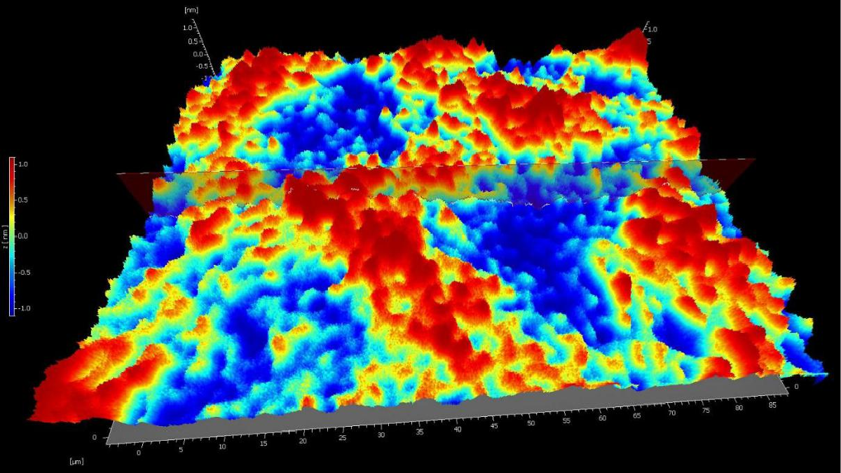
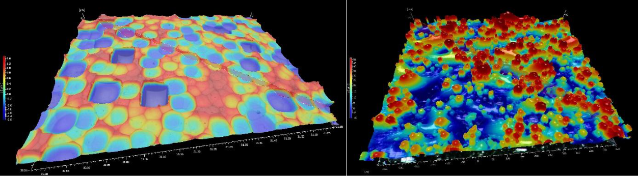
One of CSI’s standout qualities is its ability to seamlessly handle an expansive range of surface textures. For smooth, polished surfaces, the technique provides nanometer-scale height resolution, capturing even the faintest undulations and imperfections. For rough surfaces, such as those found in metal peened parts, cast materials, or 3D printed components, the broadband white-light source ensures interference contrast is preserved across steep slopes and deep valleys. This breadth of measurement capability positions CSI as a uniquely versatile tool for modern manufacturing demands.
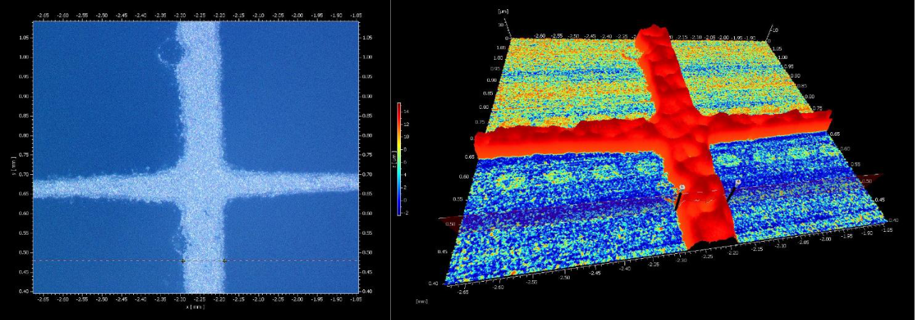
In practical terms, the CSI system scans a full field of view (FOV) in a single pass—unlike point-by-point stylus systems—and can also be configured to stitch multiple FOVs together. This data “patchwork,” powered by sophisticated stitching algorithms, creates large-area composite maps that maintain high fidelity and seamless continuity. The result is a holistic, high-resolution visualization of texture, form, and roughness over expansive surfaces.
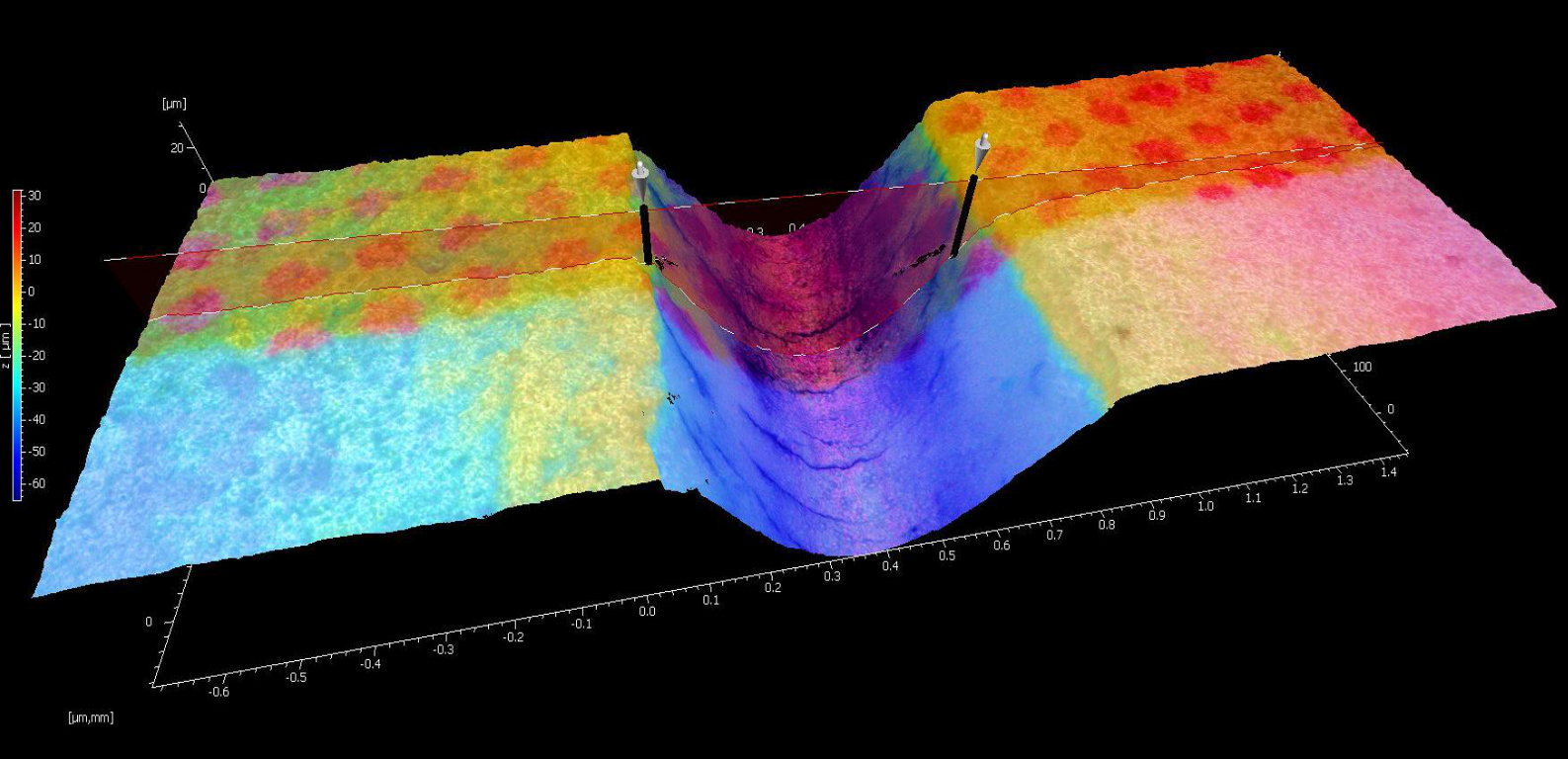
3D Metrology with True Depth and Definition
While many traditional profilometry systems provide 2D cross-sectional data, CSI offers full 3D topographical mapping. This three-dimensional view is invaluable when surface quality and uniformity are key performance indicators, such as in the manufacturing of optical components, microelectromechanical systems (MEMS), and precision coatings.
A complete 3D dataset allows engineers to analyze not just peak-to-valley roughness but also spatial distribution, areal roughness parameters, waviness, and other critical metrics that affect function and wear. With numerical data boasting sub-nanometer vertical resolution and wide lateral coverage, CSI becomes a potent tool not just for quality control, but also for research, development, and failure analysis.
In the case of surface characterization for failure investigation—where understanding material deformation, contamination, or abrasion is vital—the high-resolution, high-clarity CSI data makes it easier to pinpoint issues, compare parts, and make informed engineering decisions.
The Importance of Visual Integrity: Going Beyond Grayscale
Historically, most white-light interferometers captured grayscale image data, limiting their utility in applications where visual cues are crucial—such as tribology, where surface interactions and wear can have color characteristics, or in materials research, where phase contrast or reflectivity differences may be visually distinct.
To overcome this limitation, Polytec has innovated a method for acquiring full RGB color data by integrating three distinct light sources—red, green, and blue. This tri-color illumination system gathers detailed spectral reflectance information and overlays it with the corresponding topographic map. The resulting image is a vivid, true-color 3D representation of the surface, aligned with the actual height data.
This enhancement not only improves interpretability for the operator but also introduces a unique sensory experience that enhances defect detection and feature recognition—turning the instrument into a truly immersive metrology tool.
Material Versatility and Measurement Robustness
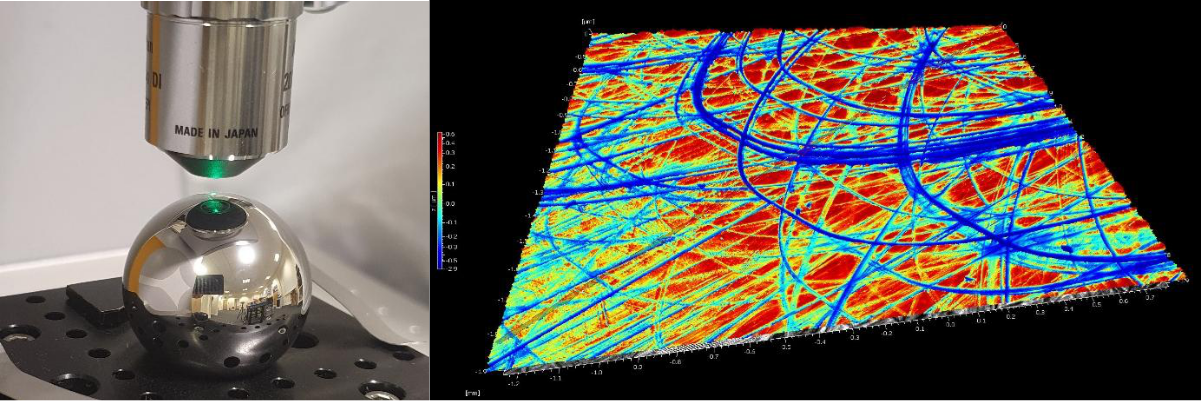
CSI’s wide adaptability to materials and finishes makes it ideal for cross-industry applications. Whether measuring the rough grain of machined steel, the polished finish of optical glass, the structured surface of semiconductor wafers, or the texture of bio-compatible polymers, the technique consistently delivers stable, high-quality data.
Reflectivity is often a limiting factor in optical measurements, yet CSI systems like those from Polytec can handle reflectivities from as low as 0.05% up to 100%, covering the spectrum from dark matte surfaces to highly reflective mirrors. Additionally, the technology performs equally well across materials with varying contrast levels, thicknesses, and optical properties.
Accelerating Throughput Without Compromising Precision
Speed and efficiency are critical in manufacturing environments, especially in production lines where inspection bottlenecks can delay output. CSI’s ability to acquire full-field measurements in a fraction of the time required by stylus-based systems makes it ideal for inline or near-line inspection scenarios. Furthermore, the CST scanning mode’s inherent Z-data determinism ensures consistency and accuracy in high-speed applications, enabling integration into automated quality control workflows.
The combination of deterministic scanning, robust stitching, color-enhanced imaging, and surface-insensitive measurement makes CSI one of the most comprehensive solutions for real-world surface metrology needs.
CSI as a Pillar of Modern Metrology
As manufacturing technologies evolve, embracing new materials, stricter tolerances, and faster production cycles, so too must the measurement tools that support them. Coherence Scanning Interferometry, and particularly Polytec’s advanced CST-enhanced implementations, represent the cutting edge of optical surface measurement.
Delivering unmatched resolution, measurement flexibility, and operational ease, CSI is not merely an incremental improvement over traditional profilometry – it is a paradigm shift. By offering deterministic, non-contact, high-speed, high-resolution 3D surface measurements with true color visualization, CSI is empowering manufacturers and researchers alike to better understand, control, and optimize the surfaces that define performance in the 21st century. Whether applied in cleanrooms, laboratories, or production lines, CSI is the tool of choice for those who demand precision without compromise.
For more information: www.polytec.com

