Phemet In-line Semiconductor Wafer Metrology Captures 16 Million Data Points Per Second
Wooptix, an innovator in semiconductor wavefront phase imaging metrology, has announced the introduction of its new Phemet metrology system that provides ultra-fast and extremely accurate wafer shape and geometry measurements with sub-nanometer resolution.
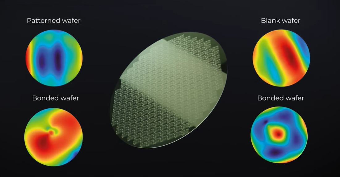
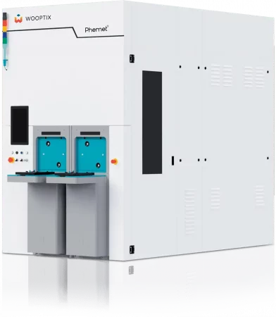 The fully automated Phemet metrology system measures the entire silicon wafer in a single image, capturing its shape and nanotopography, as well as bow, warpage and other customized parameters. It is a versatile tool that can measure blank, patterned or bonded wafers. Phemet features low noise and is vibration-resistant, enhancing the accuracy of measurements. Raw data from the system provides fab and yield engineers with comprehensive traceability to pinpoint the origin of overlay errors and other defects to enhance yield.
“Phemet addresses the growing demand for improved process control in high-volume manufacturing, especially as the industry continues to innovate with higher performance, smaller and more complex devices that involve nanoscale feature sizes and novel integration approaches”, said José Manuel Ramos, CEO, Wooptix. “The Phemet system’s ability to capture more than 16 million data points with sub-nanometer resolution with ultra speed in a single image sets a new metrology benchmark for the industry. The system is especially useful for high-throughput in-line measurements of hybrid bonding, back-side power delivery logic architectures, and next-generation 3D NAND and high bandwidth memory.”
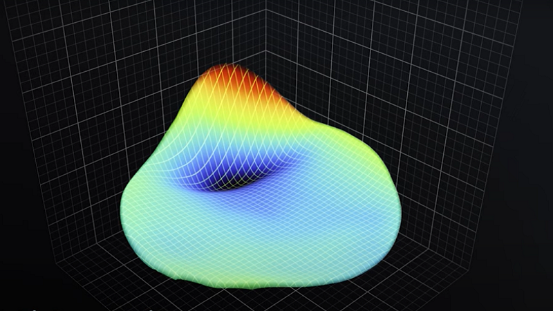
Wooptix leverages its proprietary Wavefront Phase Imaging (WFPI) technology in Phemet, which captures the wafer’s distribution of light to construct a phase map using a proprietary algorithm. WFPI quickly acquires sub-nanometer resolution wavefront phase maps with detailed information of the sample, including the wafer’s full topography and warpage. It offers ultra-high resolution at 4700×4700 pixels.
Risto Puhakka, general manager of semiconductor market analysis at TechInsights, said, “Accurate wafer shape and flatness measurements are becoming increasingly vital as semiconductor manufacturing pushes toward smaller geometries, 3D integration, and tighter process tolerances. The industry is always looking for new, innovative and high throughput metrology approaches, such as methods that combine full-field view, high-resolution, and high-speed measurements that can improve cost of process control, minimize overlay errors, and enhance overall device performance and yield.”
According to Ramos, “We have worked with tier one memory and logic customers to test Phemet and the results have been remarkable. We look forward to shipping the Phemet system to multiple key customers soon for high-volume manufacturing.”
The company will showcase Phemet at SEMICON Europa, Booth, taking place November 18-21 in Munich.
For more information: www.wooptix.com