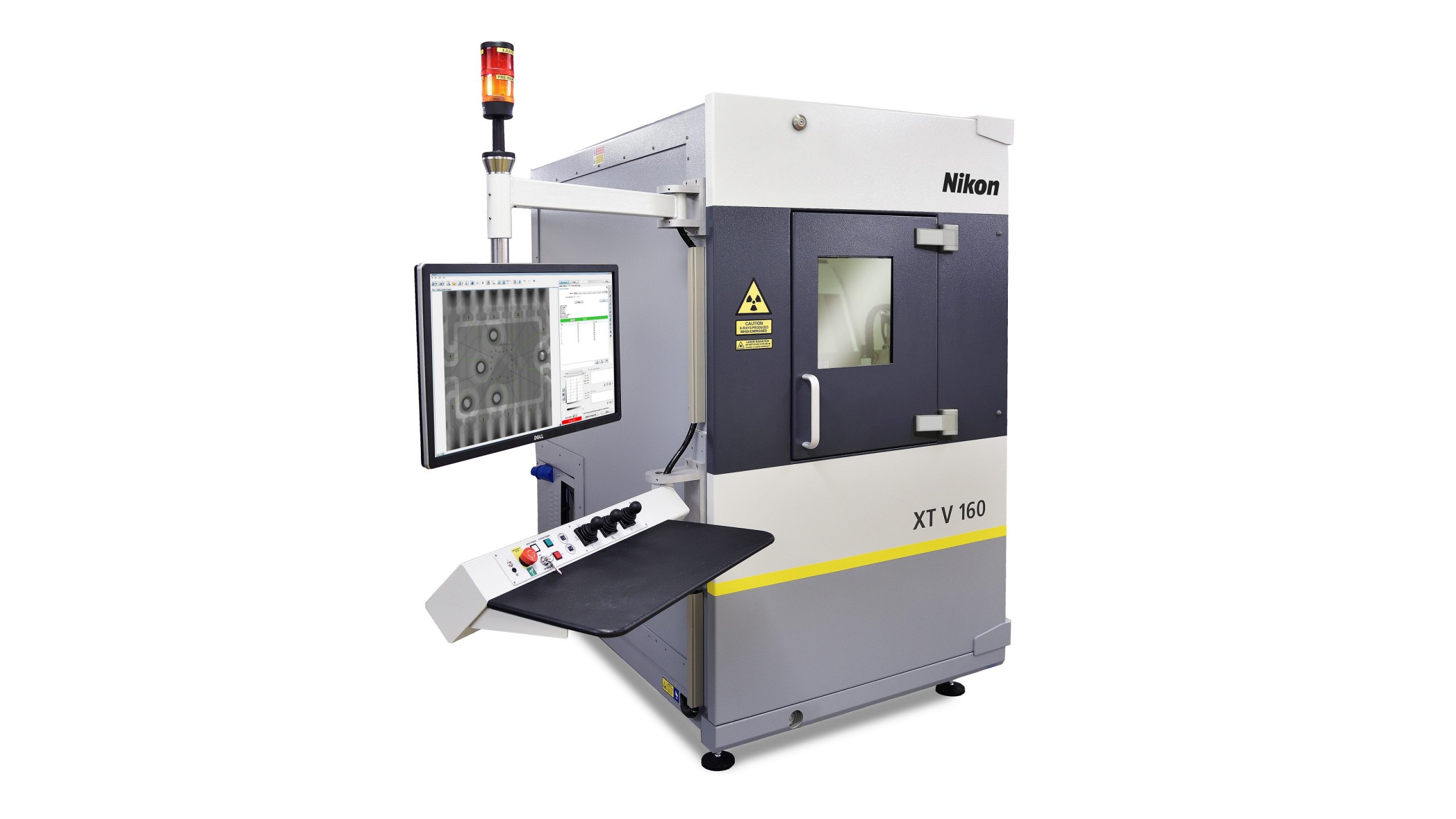
Nikon Enhances XT V for Advanced CT Inspection
Nikon Corporation has announced a comprehensive suite of enhancements to its XT V Series X-ray and CT systems, strengthening the platform’s position as a world-class solution for non-destructive inspection of electronic components. These enhancements enable operators to achieve better image quality, scan heavier samples, and protect sensitive components from electrostatic discharge and radiation damage.
One software enhancement and five hardware enhancements are available as optional upgrades to the XT V Series, allowing customers to customise their systems based on their specific application requirements.
Software Enhancement
High Contrast Filter 2.0: Offers consistently clear imaging that ensures defects are visible immediately, for any combination of sample shape and density.
Hardware Enhancements
Heavy Duty Tray: Enables larger, heavier parts to be scanned. Operators can scan more parts in each batch and expand inspection capabilities.
Diamond Window: Delivers improved image contrast across the operating range, particularly beneficial for low-density and mixed-material samples, resulting in less noise and faster
Low-Dose Collimator: Protects radiation-sensitive electronics, minimising doses to sensitive parts such as semiconductor devices while enabling safe inspection of larger batches.
ESD Safety Upgrade: Provides ESD-safe inspection of sensitive electronic components to IEC 6100-4-2, ANSI/ESD 520.20, and JEDEC JESD625 standards when installed in an ESD-Protected Area (EPA), allowing for confident integration into ESD-safe processes.
High Magnification CT Arm: Enables higher magnification CT scans for small samples, allowing operators to see finer details than previously possible.
Designed for Today’s Electronics Manufacturing Challenges
 Electronics manufacturing demands precision inspection of increasingly complex assemblies. The XT V Series provides the resolution, flexibility, and imaging power needed to detect defects in BGAs, analyse bond wire integrity, and assess semiconductor structures. With the Low Dose Collimator and ESD Safety Upgrade, manufacturers can confidently inspect sensitive components without risk of damage.
Nikon’s PCB Analysis Suite further enhances inspection capability with advanced measurement and analysis of BGAs, bond wires, plated-through holes (PTH), and complex multi-layer packages such as PoP. Automated pass/fail evaluation and reporting streamline workflows and support consistent, repeatable quality control.
The XT V Series enables detailed insights into printed circuit board assemblies, electronic components, and electrical devices through an intuitive, non-destructive inspection process. X-ray inspection accelerates throughput, improves product quality, and reduces operational costs for manufacturers and researchers alike.
Fast, Automated and Collision-Safe Operation
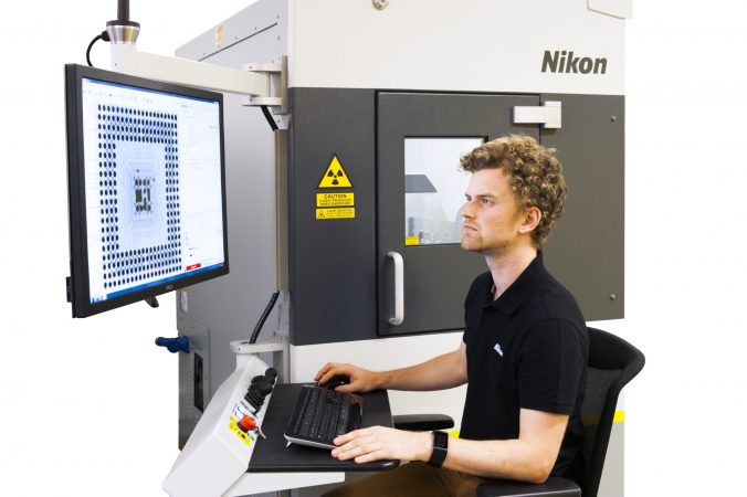
Using Nikon’s intuitive Inspect-X interface, users can set up automated inspection routines in minutes – no programming required. Automatic collision avoidance prevents physical damage to both sample and system, even at maximum magnification, while intelligent motion control ensures that regions of interest remain centralised throughout 360° sample rotation, even at extreme oblique viewing angles.
The system’s vertical configuration – featuring the X-ray source beneath the sample tray and the tilting imager above – is optimised for precision and ease of use, whether controlled through Inspect-X software or via joystick.
Superior Image Quality and Proven Reliability
Nikon’s market-leading Xi microfocus X-ray sources deliver sharp, stable, high-brightness images. Their in-house open-tube design, featuring an integral generator, ensures high reliability, low maintenance and reduced total cost of ownership.
The Diamond Window upgrade further improves contrast across the entire operating range, making even subtle defects easier to identify.
New High Contrast Filter 2.0 reveals hidden structural details by providing exceptional image quality in both high- and low-contrast regions within a single, clear radiographic image – without requiring colour adjustments. Operators can identify all aspects of a sample more quickly, improving inspection efficiency and overall throughput.
With these new enhancements, Nikon’s XT V Series continues to set the standard for high-performance X-ray and CT inspection across electronics manufacturing, semiconductor production, and advanced quality control environments – delivering unmatched clarity, flexibility and protection for today’s increasingly complex components.
For more information: industry.nikon.com