
How Semiconductor Industry Can Benefit From Automated Inspection
The semiconductor industry is a critical pillar of the modern technology landscape. The components produced are fundamental to the operation of computers, smartphones, automotive systems, and medical devices, and for countless other applications, as electronic devices are used in all modern industries.
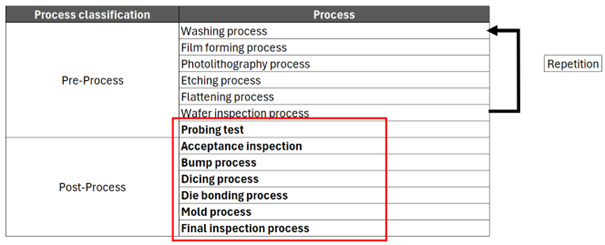
With every process step the added value of the product increases, which makes it mandatory to implement precise measurements after every stage. Early detection of the slightest deviations from the nominal shapes and values is essential so the process can be corrected.
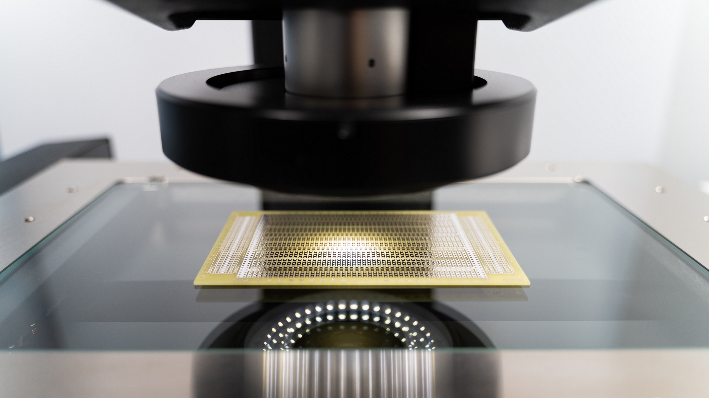
Nikon’s video measurement systems, NEXIV, are used after various process steps to control geometric parameters across the wafers. Nikon’s world-renowned optics, combined with its high-precision measurement stage, offer the perfect solution to provide the most accurate measurements of dimensions down to micrometres. By delivering high-resolution images, precise dimensional measurement, and automated quality control, these systems enhance the accuracy, efficiency, and reliability of semiconductor production. The NEXIV system comes in different stage sizes and with optical heads adjustable to the customer’s demands. Flexible illumination and optical zoom guarantee a fast, accurate, and reliable system to measure line widths down to sub-micrometre size.
Critical Dimension (CD): The NEXIV system is ideally suited to control CD measurements of various structure types and sizes across the whole wafer. The user-friendly edge detection lets the user easily create measurement programs to run automatically and generate highly repeatable and accurate measurement results, without damaging the sensitive structures. The number and position of the measurements are freely adjustable and using the quick autofocus the NEXIV system corrects for height differences across the wafer and samples to ensure a sharp image, which is the basis of precise measurement.
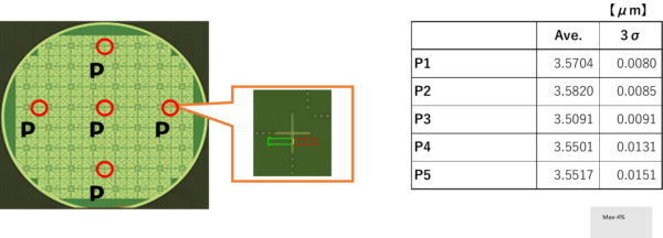
The CD structures can be in any two-dimensional form, as the NEXIV software can calculate the necessary sizes and forms and is not limited to simple point-to-point measurements. Using the 120x optical zoom a line width of 0.8 µm can be measured accurately with high repeatability. The user can freely adjust the number of measurement positions and can also program them by creating wafer maps.
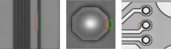
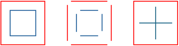
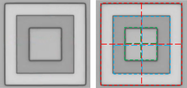
Overlay: As overlay marks can take different shapes, such as box-in-box, bar-in-bar, or cross-in-box structures, the flexible edge detection and the possibility of measuring various two-dimensional structures allow the NEXIV to accurately measure all kinds of overlay marks. Even if the overlay marks are at different heights, the world-renowned optics and the possibility of accurate autofocusing guarantee the measurement of the needed structures.
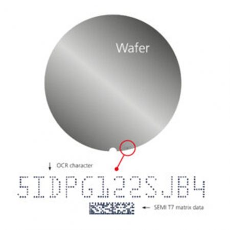
Wafer ID: The wafer ID is a Unicode code/number that is given to wafers in their bare state. The wafer ID’s position and size of the individual signs need to be accurate and follow certain SEMI standards. NEXIV’s flexible illumination, epicscopic illumination and ring light, adjust to all possible wafer surfaces from lapped & etched, grinded up to polished surfaces and generate the necessary contrast on the laser dots for the measurement. Before the wafer passes to the first lithography step, the size of the individual letters and whole ID, the position compared to the wafer centre, and the diameter and depth of the individual laser dots are thoroughly inspected. With the NEXIV, not only can the whole code be measured for all necessary parameters, such as character height, width and spacing, but also the complete code length. The position of the wafer ID to the wafer centre can be determined by accurately measuring the outer wafer edge and notch or flat.
Bumps: The most important aspects of bumps are the height, diameter, and x/y position on the chip. NEXIV’s flexible illumination consisting of an epicscopic, diascopic, and 8-segment ring light creates a perfect contrast between the bump and its surroundings. Using different head types and optical zoom, the NEXIV can be used for all bump sizes and shapes. This guarantees accurate measurement of the diameter and x/y position of the bump. Using NEXIV’s auto-focus capabilities, the user can place multiple measurement points along the wire bond and automatically evaluate the highest point.
![]()
Probe Cards: Probe cards wear off during the use and need to be controlled regularly to guarantee the correct use. With the confocal NEXIV, fast and accurate measurements of all tips can be carried out with regard to tip position (x/y), height and diameter. The different head options on the confocal NEXIV allow the measurement of tip down to a few µm tip diameter.
Automation: As the semiconductor industry strives for automation to minimize human interaction, it is crucial for customers to fully automate the NEXIV. Nikon’s own wafer loader (NWL 200) can be combined with a NEXIV to offer an easily automated wafer-handling solution. Together with external suppliers, Nikon also offers customized solutions to fulfill customers’ requirements regarding wafer sizes, end effectors, load ports, pre-aligner and filters.
For more information: www.industry.nikon.com

