Cryo-Electron Tomography Breakthrough Promises Near-Elimination of Lithography Defects
A pioneering study by a joint Chinese research team has unveiled a method that could dramatically reduce defects in semiconductor lithography, a crucial step in chip fabrication, by up to 99%. Using cryo-electron tomography (cryo-ET), researchers were able to visualize, for the first time, the microscopic causes of recurring manufacturing flaws, paving the way for more reliable and cost-efficient chip production.
The findings, published in Nature Communications on September 30, were led by Professor Peng Hailin of Peking University, in collaboration with teams from Tsinghua University and the University of Hong Kong.
Solution Compatible with Existing Production Lines
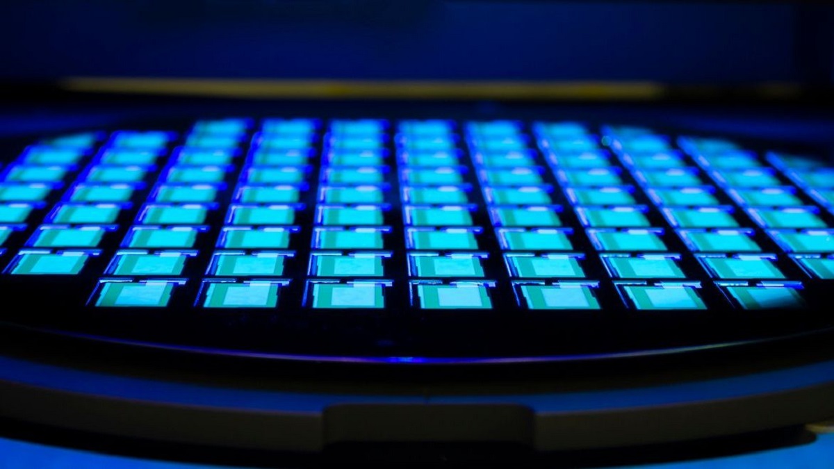
According to Peng, the method is fully compatible with current semiconductor fabrication facilities and can reduce lithography defects on 12-inch wafers by 99%, representing a significant potential cost saving. Lithography, which transfers circuit patterns onto silicon wafers, is one of the most critical stages of chip manufacturing.
The process begins with the application of photoresist, a light-sensitive coating, onto a wafer. A lithography machine projects ultraviolet or extreme ultraviolet light through a mask to expose the photoresist, followed by a development step where chemical processing reveals the intended circuit patterns. This final stage is particularly prone to defects.
“During development, dissolved photoresist molecules can reattach and entangle, forming particles that redeposit onto sensitive circuit patterns,” Peng explained. These defects, known as ‘bridging’ errors, can be catastrophic for modern chips, especially as process nodes shrink to 5 nanometers. On a single 12-inch wafer, defect counts can exceed 6,600—far beyond acceptable limits for mass production.
Freezing Molecular Motion to Reveal Hidden Flaws
To understand and mitigate these issues, the team introduced cryo-ET into semiconductor research. After standard lithography steps, the thin layer of developer containing the photoresist was rapidly frozen to -175°C, effectively ‘locking’ molecular structures in place. Multi-angle imaging then allowed three-dimensional reconstruction of the photoresist polymers in their native state.
This approach revealed that about 70% of the polymers were adsorbed at the air-liquid interface rather than dissolved in the developer. These chains formed loose entanglements that aggregated into particles 30–40 nanometers in size, which later redeposited during rinsing to create defects.
A Dual-Approach Strategy for Defect Reduction
Armed with these insights, the researchers designed a dual-pronged solution compatible with existing production lines:
Suppressing Entanglement: Slightly increasing the post-exposure bake temperature reduced polymer entanglement at the source, preventing the formation of large aggregates.
Optimizing Development: Adjustments to the developer flow ensured polymers at the air-liquid interface were completely removed, preventing redeposition onto the wafer surface.
Tests confirmed that these interventions eliminated over 99% of pattern defects on 12-inch wafers, with high reliability and repeatability.
Implications for Semiconductor Manufacturing
Beyond lithography, Peng notes that cryo-ET could transform quality control across chip manufacturing, offering insights into etching, wet cleaning, and other processes at advanced nodes. By directly observing molecular-scale interactions, semiconductor manufacturers can optimize production steps, reduce defects, and enhance yields.
As chipmakers push toward smaller geometries and tighter tolerances, this cryo-ET–based methodology offers a promising path to near-perfect lithography and more robust, cost-effective semiconductor production.