
Advanced Surface Inspection Techniques for High-Precision Manufacturing
In manufacturing today, surface integrity is as critical as dimensional accuracy. Aerospace turbine blades, orthopedic implants, and semiconductor wafers all demand flawless surface quality, where even nanometer-scale irregularities can impact safety, efficiency, or functional performance. As tolerances tighten and geometries become increasingly complex, advanced surface inspection techniques are evolving into indispensable tools for ensuring product reliability.
The Expanding Role of Surface Inspection
Traditional metrology focused on dimensional conformance, length, diameter, flatness. Today, surface texture, roughness, and defect characterization are equally essential. The introduction of the ISO 25178 standard for 3D areal surface texture has accelerated the adoption of advanced inspection, providing manufacturers with consistent frameworks for evaluating surface quality beyond simple Ra roughness values.
In critical sectors:
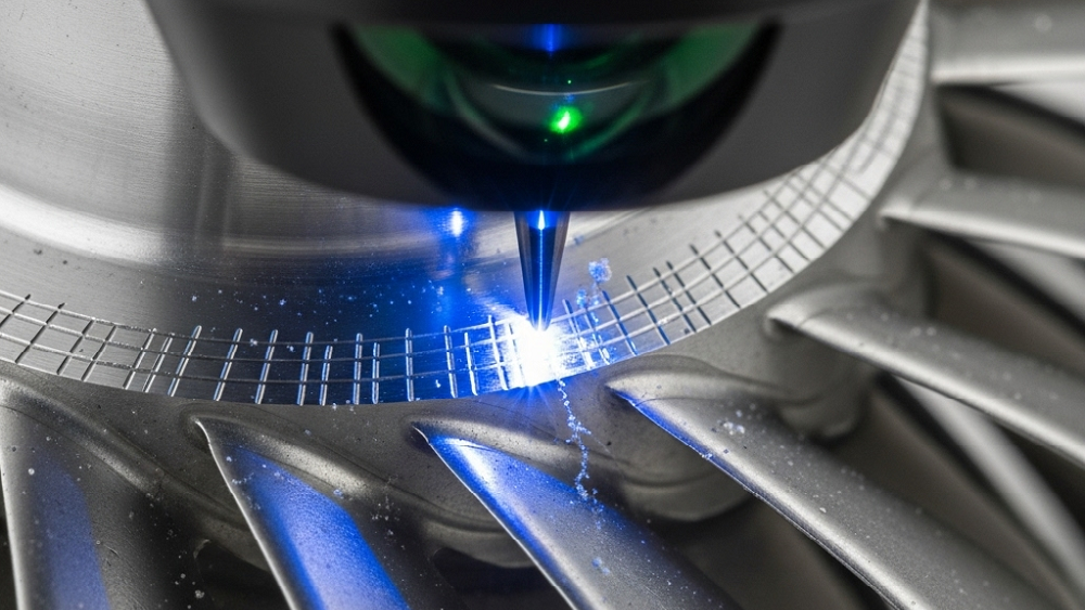
Aerospace: Tiny surface scratches on turbine blades can initiate fatigue cracks and reduce fuel efficiency.
Medical devices: Implant surfaces must balance biocompatibility and osseointegration, requiring precise micro-roughness control.
Semiconductors: Nanometer-scale surface defects can destroy yields, making ultra-precise inspection vital.
Optical Metrology: Fast, Non-Contact, and Scalable
Optical techniques dominate high-precision surface inspection because they combine speed with non-contact accuracy.
White Light Interferometry: Provides nanometer vertical resolution, ideal for smooth or reflective surfaces such as wafers and lenses.
Confocal Microscopy: Enables detailed 3D surface reconstructions, widely used in medical implant inspection.
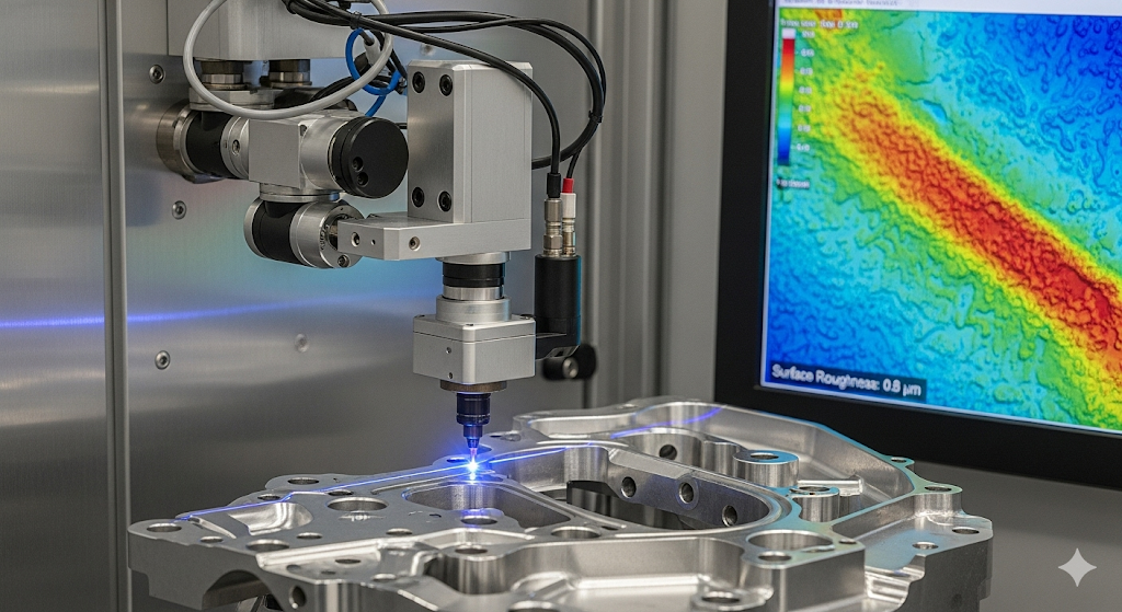
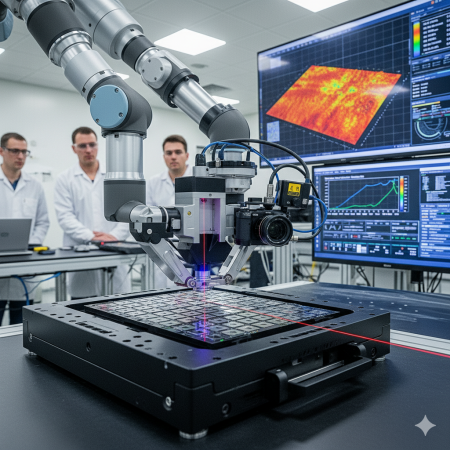
Structured Light and Laser Scanning: Deliver rapid, inline-compatible surface mapping for machined and cast components.
Optical inspection not only detects topography but also correlates surface texture with functional performance, such as friction, wear, or coating adhesion.
X-Ray and Electron-Based Methods for Deep Insights
When subsurface or ultra-fine resolution is required, electron and X-ray methods provide unmatched detail:
Scanning Electron Microscopy: High-magnification analysis of cracks, porosity, and coating defects, crucial in microelectronics.
X-Ray Computed Tomography: Initially used for internal porosity, XCT now supports precise surface reconstruction—particularly for additive manufacturing (AM) parts where both internal and external features must be validated.
Although typically slower and lab-based, recent advances in accelerated reconstruction algorithms and robot-integrated SEM/XCT setups are pushing these methods closer to inline feasibility.
AI and Machine Vision: From Detection to Prediction
Machine vision has long been used for surface inspection, but the integration of AI and deep learning is transforming its role:
Adaptive Defect Detection: AI models distinguish between cosmetic blemishes and functional defects, reducing false positives in industries like automotive.
Real-Time Monitoring: Inline AI vision systems detect surface deviations during production, feeding data back to machine tools for automatic corrections.
Predictive Analytics: By analyzing surface variation trends, AI helps predict when machining parameters will drift out of spec—transforming inspection into a proactive tool for process optimization.
For instance, in semiconductor fabs, AI-driven optical inspection has cut wafer scrap by identifying process drifts before catastrophic yield loss occurs. No single inspection technique can solve every challenge. Manufacturers increasingly adopt hybrid systems, integrating tactile, optical, and X-ray data into unified platforms.
Inline, Real-Time Surface Inspection: The Next Frontier
The ultimate goal is zero-defect manufacturing with inline inspection systems that operate at production speeds. Advances in high-speed cameras, multi-sensor platforms, and AI-powered data processing are making this feasible. Inline surface inspection not only improves quality but also transforms inspection into an active element of process control.
 Advanced surface inspection is rapidly evolving from a specialized quality gate into a core enabler of smart manufacturing. By combining optical, X-ray, and AI-driven vision systems within hybrid platforms, industries can ensure both dimensional accuracy and surface integrity at unprecedented levels. As inline, intelligent, and predictive inspection systems mature, manufacturers are moving closer to a future where defects are not just detected—they are prevented in real time.
In high-precision manufacturing, every micron counts, and surface inspection is proving to be the critical differentiator between compliance and competitive advantage.
Technology Provider Spotlight
Several leading technology providers are shaping the future of advanced surface inspection:
Bruker – pioneers in white light interferometry and 3D optical surface metrology, with systems widely used in semiconductor and medical applications.
Zeiss – offering a broad portfolio including confocal microscopy and X-ray CT for industrial inspection, enabling multimodal hybrid measurement solutions.
Keyence – delivering high-speed inline optical profilers and vision systems optimized for production environments.
Nikon Metrology – providing high-resolution X-ray CT scanners tailored for additive manufacturing and aerospace applications.
Hexagon Manufacturing Intelligence – integrating optical scanning, multisensor metrology, and AI-driven data platforms for smart manufacturing workflows.
These innovators are enabling manufacturers to integrate surface inspection into the digital thread, ensuring that data collected at the surface level feeds directly into predictive quality control, process optimization, and lifecycle product management.
Author: Gerald Jones Editorial Assistant

